This sim moves the simple Middlebrook gain probe to the “inner” feedback loop, measuring all of the gain around the output stage
I think you can see it is a much more useful way to view the stability margin of TMC
To look at the phase margin numbers with the added delay we have to convert the delay time into phase – since delay has linear phase with frequency the phase depends on the frequency
For the CMC loop 100 nS delay at the 977KHz gain intercept is:
100ns * 977kHz * 360 degrees = 35 degrees added phase shift
the cursor reading gives 77.8 degrees phase margin for the CMC at 0 delay,
42.6 degrees at 100 ns (append @5 to both V in the waveform formula, ie V(d_cmc)@5/V(b_cmc)@5)
77.8 - 35.2 = 42.6 which agrees with the idea that the added delay is a fair measure of phase margin
the numbers clearly don’t work so neatly in the outer loop gain/phase plot of TMC because the gain intercept is a moving target
the Inner loop Bode gain/phase measurement of TMC below Is well behaved and we can do the same calculation:
100ns * 1.69MHz * 360 = 60.8 degrees added phase shift
the cursor reading gives 58.7 degrees phase margin for the CMC at 0 delay,
-2 degrees at tau = 100 ns, step 5
58.7 – 60.8 = -2.1 which again agrees and predicts that the TMC loop will be unstable with 100 ns added delay – as the tran sim pic above shows
as a further check note that 100nS is just over the 0 degree line and the previous step at 75ns delay has poor but positive phase margin – and the tran sim shows it does settle out instead of oscillate
(Thanks to Mike Engelhardt of Linear Technology – you may have noticed the stepped waveform colors didn’t agree in the previous post Bode plot but they do match in this sims pic – the 1st time I’ve had a bug fixed over lunch! )
I assume anyone wanting to verify can mod the .asc in my previous post
A first question: I do not understand why in the simple Miller loop, with the values given, the loop transmission crossover frequency is not 10Mhz/16 =625 Khz instead of 1 Mhz.
Thanks
JPV
because you missed the doubling of the diff pair gain by the mirror?
2*(1/(2*(470 Ohm + 26 mv/0.5 ma))) ~= 1/500 mho
with ~15 pF Cdom ~= 20 MHz GBW
then with the beta of 1/20 pretty much gives the observed 1 MHz corner freq
for more fun with my delay sim you can edit both circuits to TMC and measure the outer loop gain in one and inner loop gain in the other
the final 100 ns delay step @5 gives very close to the same `1.7 MHz intercept and -2 to -4 degrees phase margin - so you could say measuring the outer loop gets you the same stability result if you add delay externally - it just doesn't help you predict the stability limit from the 0 delay plot
a good question is why the resistance to measuring the inner loop?
Probably because we expect just measuring the outer loop to be right from experience with 1st order loops as in the CMC case
there are complex rules for measuring multiloop circuit stability by "loop cutting" methods - the simplest is that measuring the global outer loop gain/phase margin is sufficient if all internal loops are negative feedback and are stable - I think the "fail" is that TMC is a positive feedback loop - admittedly expected to be stable if the output stage gain is less than unity
I think the probe position in my sims is adequate because it breaks both the global and local output stage feedback at the same time and the remaining “inner” miller feedback around the VAS is negative feedback and stable
to anticipate a possible objection - the delay element could be put in-between the driver and output Q with little effect on the result if you just like the visual appearance of not modifying feedback component connections
the delay following the output Q and RL is probably a little better since the pre/driver see the output Q's base load - I don't know how to make a "reciprocal" delay
Last edited:
Hi, Bob
In fact, a cap as low as 0.2pF is enough to get rid of the TPC OL gain
peaking, so in real implementation, it s unprobable that such peakings
occur as the parasistic layout and components leads caps are enough to
create this cap, while not decreasing available gain.
Though, as soon as the loop is closed, the usual step response
peaking will remain, since the TPC loop becomes then dominant.
As i already pointed, a TMC network pondered with a TPC one
is generaly the optimmum in respect of the global behaviour,
although i m not still sure if there isnt undesirable by products.
cheers,
w
Hi wahab,
The amount of bridging capacitance needed to suppress the loop gain peaking will of course be highly dependent on the particular design. 0.2pF was not enough to do it in my design. Other designs, which use higher overall values of compensation capacitance will need even more bridging capacitance. Of course, a design that does not use an emitter follower in front of the VAS transistor will typically not need the bridging capacitor because that function will be performed by the collector-base capacitance. But I don't think we are talking about such low-performance designs here.
I would not leave the bridging capacitance to chance. In fact, I think a decent layout would not have anywhere near 0.5 pF (or even 0.2 pF) from the VAS collector to the input of the emitter follower feeding the VAS transistor. On the other hand, one could do the calculations and deliberately create some PWB inter-trace capacitance to fulfill the role of C3.
Could you clarify your statement:
"As i already pointed, a TMC network pondered with a TPC one
is generaly the optimmum in respect of the global behaviour,
although i m not still sure if there isnt undesirable by products."
Cheers,
Bob
because you missed the doubling of the diff pair gain by the mirror?
2*(1/(2*(470 Ohm + 26 mv/0.5 ma))) ~= 1/500 mho
with ~15 pF Cdom ~= 20 MHz GBW
then with the beta of 1/20 pretty much gives the observed 1 MHz corner freq
for more fun with my delay sim you can edit both circuits to TMC and measure the outer loop gain in one and inner loop gain in the other
the final 100 ns delay step @5 gives very close to the same `1.7 MHz intercept and -2 to -4 degrees phase margin - so you could say measuring the outer loop gets you the same stability result if you add delay externally - it just doesn't help you predict the stability limit from the 0 delay plot
a good question is why the resistance to measuring the inner loop?
Probably because we expect just measuring the outer loop to be right from experience with 1st order loops as in the CMC case
there are complex rules for measuring multiloop circuit stability by "loop cutting" methods - the simplest is that measuring the global outer loop gain/phase margin is sufficient if all internal loops are negative feedback and are stable - I think the "fail" is that TMC is a positive feedback loop - admittedly expected to be stable if the output stage gain is less than unity
I think the probe position in my sims is adequate because it breaks both the global and local output stage feedback at the same time and the remaining “inner” miller feedback around the VAS is negative feedback and stable
to anticipate a possible objection - the delay element could be put in-between the driver and output Q with little effect on the result if you just like the visual appearance of not modifying feedback component connections
the delay following the output Q and RL is probably a little better since the pre/driver see the output Q's base load - I don't know how to make a "reciprocal" delay
Hi jcx,
My understanding and sims do not indicate the the inner loop around the output stage is a positive feedback loop. This is the loop that starts at the output of the amplifier, passes through R1, and gets to the input of the VAS through C1. Although C2 is connected to the input of the output stage and to the output of the VAS, it provides less transmission to the output stage than the path through C1. If you open the global loop, and also open the local loop at R1, then apply a signal to R1, you will see the loop gain of the local loop.
You are certainly correct that just looking at the global loop is insufficient. The total amount of feedback enclosing the output stage derives from two paths, one the global feedback path and the other the local loop path. The sum of the loop signals of both of these paths is what causes the output stage to be enclosed by the feedback that has the peak and typically has a higher gain crossover frequency.
Cheers,
Bob
Hi wahab,
Of course, a design that does not use an emitter follower in front of the VAS transistor will typically not need the bridging capacitor because that function will be performed by the collector-base capacitance. But I don't think we are talking about such low-performance designs here.
Cheers,
Bob
Please remember, there is more than one road to Rome.
Please remember, there is more than one road to Rome.
Hi Stinius,
This is certainly true, but it is only my opinion that before one applies TPC or TMC to get really high performance out of a design, they should have at least given the design a decent VAS (with an emitter follower in front of it, what we often call a Darlington VAS). Just my opinion on priorities, and others may of course differ.
Cheers,
Bob
stability test
Hi jcx,
I'm not sure if you consider me part that 'engineering oriented community', but years ago I already said that any compensation trick (and even HEC) that lowers the distortion, has an impact on the stability. So I fully endorse the TANSTAAFL principle.
Referring to post 1106, where I stated that TMC is essentially a 1st order system, that is, at least with idealized components, your output conductance sim becomes pointless, as the output impedance is zero.
(just teasing a bit)
Till now, I ran similar stability tests by means of a capacitor (5...100nF) directly tied to the output and gnd. Together with the lead or trace inductances, additional poles were created. It appeared that, compared to CMC, TMC amps becomes already unstable with smaller caps.
However, your stability test, using a simple delay, provides less ambiguous results, as it doesn't rely on inductances, which may vary from amp to amp. IOW, it's more 'robust'.
Cheers,
E.
I don't suppose a direct sim of robustness to added output delay will cause anyone to rethink?
As I stated earlier in this thread a sticking point seems to be people wanting to believe that the outer loop gain/phase margin Bode plot of TMC looking like CMC means you managed greater loop gain/distortion reduction - "for free"
I find it hard to believe the resistance to the TANSTAAFL principle among a engineering oriented community
Hi jcx,
I'm not sure if you consider me part that 'engineering oriented community', but years ago I already said that any compensation trick (and even HEC) that lowers the distortion, has an impact on the stability. So I fully endorse the TANSTAAFL principle.
Specifically I have pointed to Bode's Integral relations and BJ Lurie's work that shows how this "conservation law" for feedback is applied
My earlier output conductance sim clearly established that the added feedback is externally visible - simply by "tugging" on the output node you can tell TMC from CMC
the Bode Integral relations lead me to expect more feedback has a cost in loop gain slope and phase margin - the extra distortion reduction performance of TMC - is not "free"
Referring to post 1106, where I stated that TMC is essentially a 1st order system, that is, at least with idealized components, your output conductance sim becomes pointless, as the output impedance is zero.
(just teasing a bit)
Now I have another sim - this time I packaged up Bob's amp, bringing out the VAS connections so compensation can be seen as external components
I've added a pure delay to the output of the amp - between the loaded output and the normally output connected feedback components to sim variable "excess poles" - which Bob mentions in his book can be approximated as delay.
[snip]
In sum: You Have been bitten by those inner loops - TMC is not as stable as CMC, the gain/phase measured in the outer loop is not informative in the TMC case
Till now, I ran similar stability tests by means of a capacitor (5...100nF) directly tied to the output and gnd. Together with the lead or trace inductances, additional poles were created. It appeared that, compared to CMC, TMC amps becomes already unstable with smaller caps.
However, your stability test, using a simple delay, provides less ambiguous results, as it doesn't rely on inductances, which may vary from amp to amp. IOW, it's more 'robust'.
Cheers,
E.
because you missed the doubling of the diff pair gain by the mirror?
2*(1/(2*(470 Ohm + 26 mv/0.5 ma))) ~= 1/500 mho
with ~15 pF Cdom ~= 20 MHz GBW
then with the beta of 1/20 pretty much gives the observed 1 MHz corner freq
I didn't miss that. Simply I took the 30 pF of Bob's book instead of your 15which gives as GBW: gm/(2pi C) = 1/ 500 2 pi 30 ) = 10Mhz.
I read on your shematic a resistor of 3000 instead of 2000 which gives a beta of 16 instead of 20, therefore my mistake
Thanks for the answer.
abstruse or obtuse? I suspect we'll continue having it both ways
I really hope to avoid math but the wye-delta transformation of the TPC, TMC network does seem promising for some insight when interpreting the mixed feedback loop of VAS, OP in TMC - as long as we can deal with FNDR elements in feedback loops
I haven’t been able to install MathCad 11 (the only version to use, the last with the Maple Symbolic engine) on my Vista machine so I may be slow to fire up the old offline computer with the lousy monitor… that would require moving from the only comfy chair in the house
Guys,
I am following your stellar discussions with great interests. All those discussions are great but I really wonder if the thread is the good one.
I realize that a lot of usefull information is hidden in the middle of thread with non relevant tittles.
All I can conclude is that if the thread tittle contains the word "Bob", than there should be some usefull information?
Why not a thread to summurize the conclusions about TPC, TMC, ETMC... I am never sure I have the latest updates.
Could you clarify your statement:
"As i already pointed, a TMC network pondered with a TPC one
is generaly the optimmum in respect of the global behaviour,
although i m not still sure if there isnt undesirable by products."
Bob
Some sims i posted by there clearly show that TMC has higher
undesirable frequency products in 19+20khz IMD for the 1KHZ
product and subsequents 18 and 21khz products.
Edmond suggested the IPS non linearity due to increased output
current from this latter in case of TMC higher IPS loading.
I still do not agree with this explanation, as i provided a sim
that show that reducing the IPS degeneration yield a reduction
of all IMD products safe the one mentionned, meaning that the
increased available NFB indeed act on part of the signal while
being totaly inneffective for the 1KHZ, 18 and 21khz products.
Increasing the VAS gain AND slew rate by reducing the cap that
goes to its input effectively reduce those reluctants products,
meaning that VAS+OPS slew rate is the cause of this distorsion.
Indeed, IMD appear when a fast system drive a slower one.
As a cure, one has to increase the slew rate and subsequently
the VAS gain at about 20khz, and in this respect, the best is to use
a mix of TMC and TPC, that is connecting the TPC and TMC resistors
to ac ground and output respectively, as usual.
Adjusting the ratio of the two resistors will allow to transit from
pure TPC compensation to pure TMC one.
We can then choose an equilibrium that yield limited overshoot
while retaining the TMC better usage of local NFB (better thd reduction)
for the inevitably gain dumping VAS compensation.
Moreover, this allow to use a very light phase lead compensation
to completely suppress the TPC influence induced overshoot, rather than
an oversized one in case of TPC alone.
As a separate topic, a few remarks about your sim schematic.
Why using slow power devices ?..
Why a triple EF since sims show that it doesn t bring better perfs?
Last but not least, the compensation caps seems to me quite
optimistic considering how low their values are, even counting
the heavy IPS degeneration.
cheers
w
Last edited:
sorry for being unclear, .
WuGit,
Be assured that we didn t expect it being otherwise,
so no need to be sorry, you re pardonned from the start..
Some sims i posted by there clearly show that TMC has higher
undesirable frequency products in 19+20khz IMD for the 1KHZ
product and subsequents 18 and 21khz products.
Edmond suggested the IPS non linearity due to increased output
current from this latter in case of TMC higher IPS loading.
I still do not agree with this explanation, as i provided a sim
that show that reducing the IPS degeneration yield a reduction
of all IMD products safe the one mentionned, meaning that the
increased available NFB indeed act on part of the signal while
being totaly inneffective for the 1KHZ, 18 and 21khz products.
Increasing the VAS gain AND slew rate by reducing the cap that
goes to its input effectively reduce those reluctants products,
meaning that VAS+OPS slew rate is the cause of this distorsion.
Indeed, IMD appear when a fast system drive a slower one.
As a cure, one has to increase the slew rate and subsequently
the VAS gain at about 20khz, and in this respect, the best is to use
a mix of TMC and TPC, that is connecting the TPC and TMC resistors
to ac ground and output respectively, as usual.
Adjusting the ratio of the two resistors will allow to transit from
pure TPC compensation to pure TMC one.
We can then choose an equilibrium that yield limited overshoot
while retaining the TMC better usage of local NFB (better thd reduction)
for the inevitably gain dumping VAS compensation.
Moreover, this allow to use a very light phase lead compensation
to completely suppress the TPC influence induced overshoot, rather than
an oversized one in case of TPC alone.
As a separate topic, a few remarks about your sim schematic.
Why using slow power devices ?..
Why a triple EF since sims show that it doesn t bring better perfs?
Last but not least, the compensation caps seems to me quite
optimistic considering how low their values are, even counting
the heavy IPS degeneration.
cheers
w
Hi wahab,
I think the 19+20 kHz sims are a good further way to look at performance of TPC vs TMC. As you know, I'm a big believer in 19+20kHz CCIF. I just haven't gotten around to do any of my own on this topic yet. As I pointed out earlier, the comparative results of the CCIF IM approach may not track those of the THD approach because of the frequency dependence of NFB loop gain. A compensation approach that offers substantially more loop gain at frequencies in the range of 20 kHz will tend to better suppress the CCIF IM sidebands.
The power devices I used in my sim are among the most popular power devices out there that are not of the really high-speed types. They provide a good baseline for typical amplifier design, with their ft in the neighborhood of 6 MHz.
I believe that triple output stages virtually always deliver a better amplifier. That is why I chose them for the example I have been showing. One could just as easily ask why I did not choose to use a CFP output stage. I think this is just a "to each his own" question. BTW, bear in mind that my amplifier example is driving a 4 ohm load with a single pair.
The compensation caps were simply chosen to yield a conventional Miller-compensated amplifier with a 1 MHz gain crossover. I don't think that is terribly optimistic, especially given the phase and gain margins that numerous sims have shown here. The caps may seem small, but you really need to look at the transconductance of the input stage as well. The tail current is only 1 mA, with each emitter degenerated by a factor of 10:1 with a 470 ohm resistor. You just may not be used to seeing designs with such an input stage. If the stage was run with a 4 mA tail current, and degeneration kept at 10:1, transconductance would have increased by a factor of four and you would see compensation capacitor values 4 times higher.
Cheers,
Bob
Some sims i posted by there clearly show that TMC has higher undesirable frequency products in 19+20khz IMD for the 1KHZ
product and subsequents 18 and 21khz products.
Edmond suggested the IPS non linearity due to increased output current from this latter in case of TMC higher IPS loading.
I still do not agree with this explanation, as i provided a sim that show that reducing the IPS degeneration yield a reduction of all IMD products safe the one mentioned, meaning that the increased available NFB indeed act on part of the signal while being totally ineffective for the 1KHZ, 18 and 21khz products.
Increasing the VAS gain AND slew rate by reducing the cap that goes to its input effectively reduce those reluctant products, meaning that VAS+OPS slew rate is the cause of this distortion. Indeed, IMD appear when a fast system drive a slower one.
[snip]
cheers
w
Hi Wahab,
Firts, my apologies for not responding to your previous post. For some reason I missed it.
What do you mean by "safe the one mentioned" ? Probably "except the one mentioned" (i.e. 1, 18, 21kHz), right?
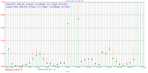
Anyhow, I got different results from slightly different circuits. The compensation components are as follows:
TMC: C1=120pF, C2=600pF, R1 = 530R
TPC: C1=600pF, C2=120pF, R1 = 530R (Harry's style)
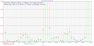
Opposed to previous sims, with these arrangements the IMD products of TMC are equal or lower compared to TPC (1st pic). But in other cases they could be higher due to a higher load of the IPS (the devil is in the detail). This can be remedied by increasing the tail current, which makes the IPS more linear, see 2nd pic. Indeed, the IMD is lower now.
However, due to a higher tail current, one might argue that the higher slew rate attributed to better IMD figures. So I lowered the tail current to its original value and linearized the IPS in another way: by means of Sziklai pairs. Also in this case, IMD figures are better (3rd pic). Therefore, I still believe that the IPS caused more IMD as shown in previous sims. BTW, also notice that the 'reluctant' components are reduced as well.
Cheers,
E.
Attachments

4times the LTP tail current requires 4times the value of compensation capacitance !If the stage was run with a 4 mA tail current, and degeneration kept at 10:1, transconductance would have increased by a factor of four and you would see compensation capacitor values 4 times higher.
Is this in the book?
I intended to re-read many chapters. Looks like compensation chapters must be the first.
yes, the different LTP current would require a different emitter resistor value for the same degeneration.
Bob quotes this 10x degeneration quite a lot.
What are the pros and cons of different amounts of degeneration in each of the various stages.
I assume it does not have to be 10x in the LTP, nor in the VAS, nor in the driver, nor in the output devices.
Where suits less and where suits more and what is lost when one adopts a higher or lower degeneration?
Last edited:
- Home
- Amplifiers
- Solid State
- Bob Cordell's Power amplifier book