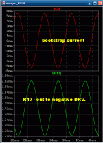
r16=4k7 for +-70Vdc????
R18=4k7?
Works perfect ...Andrew. The ones I have now are 2.7/2.7K , exact circuit , 45-0-45V. To keep the 7ma VAS standing current , the 4.7K's are needed. (See below 75-0-75VDC / 4.7k)
Edit - I see the error R17-18 are the 4.7k's

OS
Attachments
Last edited:
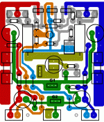
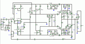
At it again , after a break.  (Pix 1) is the NEW PB60LP low profile for those with "IDI BIDI" amplifier cases , it will be done tomorrow. Also for tomorrow , I should have the NEW IMPROVED PB60 / PB250 done. NOTHING was wrong with the last ones.But after testing , research , and discussion... 2 ground points are the best for these boards.
And here is why .... PMA pointed out that large rail caps on the main board increase noise and foul up the star with their "filthy" current pulses. I LIKE big onboard rail caps for the simple reason that they negate the effects of the FUSE!! (yes, the fuse is a resistor) and they add a noticable "edge" to the sound. SO , why not just have their ground separate and feed that individually back to the main star of the amp's power supply. IT works , On the "supersym" , it halved my already low noise floor ... a worthwhile design change.
Andrew T. advised on "guard rings" and taking negative feedback in the most pure form back to the differential. This is now the "standard" (a shielded cable with the shield at the same potential as the NFB signal) coming direct from the inductor to the voltage boards NFB input.
And , the "biggie" Greg erksine informed me of the miswired "doug self magic resistor" on the onboard Vbe. This has been corrected. Anybody that has made the PB250/60 could just jumper (omit) that resistor anyways. BELOW are all 3 boards with all 3 "fixes". Tomorrow night they will be all ZIPPED and ready to go.
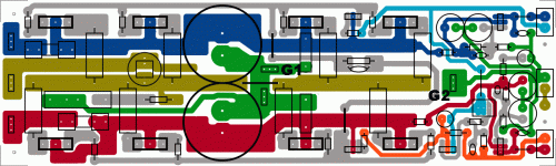
G1 and G2 - G1 is the "dirty ground" ,accepts loudspeaker return and goes back to the main PS star with 12 or 14 ga. wire. G2 is the "clean" ground , it is only a reference for the C/R/C filter - capacitance multiplier as well as the voltage board ground. IT only needs a 18 Ga. wire returned to the PS main star.
ALL BOARDS color code .. GREEN = both grounds/ RED=V+ / BLUE=V- /YELLOW= signal paths /ORANGE=positive drive / Light BLUE= neg. drive...
ALSO , next to come is the PB200M , which will be a quasi MOSFET 4 device masterpiece to round out the power board lineup. (last pix)
OS
(Pix 1) is the NEW PB60LP low profile for those with "IDI BIDI" amplifier cases , it will be done tomorrow. Also for tomorrow , I should have the NEW IMPROVED PB60 / PB250 done. NOTHING was wrong with the last ones.But after testing , research , and discussion... 2 ground points are the best for these boards.And here is why .... PMA pointed out that large rail caps on the main board increase noise and foul up the star with their "filthy" current pulses. I LIKE
big onboard rail caps for the simple reason that they negate the effects of the FUSE!! (yes, the fuse is a resistor) and they add a noticable "edge" to the sound. SO , why not just have their ground separate and feed that individually back to the main star of the amp's power supply. IT works , On the "supersym" , it halved my already low noise floor ... a worthwhile design change.Andrew T. advised on "guard rings" and taking negative feedback in the most pure form back to the differential. This is now the "standard" (a shielded cable with the shield at the same potential as the NFB signal) coming direct from the inductor to the voltage boards NFB input.
And , the "biggie" Greg erksine informed me of the miswired "doug self magic resistor" on the onboard Vbe. This has been corrected. Anybody that has made the PB250/60 could just jumper (omit) that resistor anyways. BELOW are all 3 boards with all 3 "fixes". Tomorrow night they will be all ZIPPED and ready to go.
G1 and G2 - G1 is the "dirty ground" ,accepts loudspeaker return and goes back to the main PS star with 12 or 14 ga. wire. G2 is the "clean" ground , it is only a reference for the C/R/C filter - capacitance multiplier as well as the voltage board ground. IT only needs a 18 Ga. wire returned to the PS main star.
ALL BOARDS color code .. GREEN = both grounds/ RED=V+ / BLUE=V- /YELLOW= signal paths /ORANGE=positive drive / Light BLUE= neg. drive...
ALSO , next to come is the PB200M , which will be a quasi MOSFET 4 device masterpiece to round out the power board lineup. (last pix)
OS
Attachments
post302,
careful with the use of "magic" for that extra Vbe multiplier resistor.
There is another paper (can't remember the Author) on introducing a "magic" resistor into the topology to improve the sound quality. It is quite different from the multiplier's extra resistor.
R80 is still in the wrong place.
The driver is tapped into the bottom of R80 adjacent to the Vbe transistor's collector.
As a result the capacitor must now be moved to the VAS side of the multiplier. C86 connects the collector of Q8 (VAS) to the collector of Q10 (CCS)
Last edited:
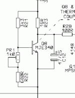
And to help compensate for the capacitance of the lower outputs, how about trying a small cap parallel to R88, equal to the capacitance seen by Q99?
Also the MJE3x0 drivers seem a little low-Fi...? Especially since everything else is high-tech japanese devices?
- keantoken
Also the MJE3x0 drivers seem a little low-Fi...? Especially since everything else is high-tech japanese devices?
- keantoken
post302,
careful with the use of "magic" for that extra Vbe multiplier resistor.
There is another paper (can't remember the Author) on introducing a "magic" resistor into the topology to improve the sound quality. It is quite different from the multiplier's extra resistor.
R80 is still in the wrong place.
The driver is tapped into the bottom of R80 adjacent to the Vbe transistor's collector.
As a result the capacitor must now be moved to the VAS side of the multiplier. C86 connects the collector of Q8 (VAS) to the collector of Q10 (CCS)
I did not update the schema , the boards reflect the change, although.
I get the hard part first (the boards), then go back do "cleanup" (match BOM , schema, parts overview...). Also , I reuse previous simulator builds to make new ones... 
"Magic resistor" AHHHH 1
I almost forgot, To eliminate or reduce the "memory effect" the french dude put them between active and cascode trannies. (a GX amp update
). Link is here : Memory Distortion Philosophies - Part 5 : Circuits, continuedBy keentoken - And to help compensate for the capacitance of the lower outputs, how about trying a small cap parallel to R88, equal to the capacitance seen by Q99?
Also the MJE3x0 drivers seem a little low-Fi...? Especially since everything else is high-tech japanese devices?
You don't like MJE340/350's ....
those poor , poor devices , nobody likes them .. except tube guys Would you suggest the KSA/KSC's , so the IRF's could "sing" better at 4 mhz ?? I will try Q99..OS
What is C85 for?
- keantoken
At 20k , C85 improves stability of the Vbe , reducing Xover point deviation to under 1mV on all the PB's. Still researching WHY?
OS
you're forgiven.
Nobody can do everything at the same time.
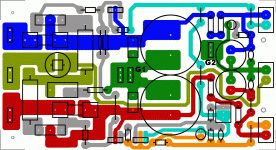
Just to lay it to rest.. is this (pix) the correct way. (reflects the boards)
OS
Attachments

c89 is in the wrong place.
It should be between the VAS and it's load (the CCS or bootstrap)
I wonder if that accounts for the very high current in the cap when the sim modeled behaviour?
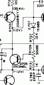
I got that (below) right from Mr. self's book ???
(Page 303 D. Self 1988).OS
Attachments
you are right.
That is what Self shows.
All I can say is that intuitively it seems more right to couple VAS to it's load. I have no evidence.
It does seem to still be coupled to it's load , just through a 10-16R resistor. The self example is the only correct one (he shows 3 examples in the book) out of over 500 examples of Vbe's in my schematic collection. Many have NO CAP at all , and if the wiper breaks in the adjustment... POOF!! mine would just become grossly underbiased . Poor designs
(example pix1)He says the 10-20R resistor "offers first order cancellation of Vbias variations due to current changes".
Changing the value of this resistor changes the correction voltage of the VBE in response to the current changes. Mr. self , using coincidentally , a 6ma current source ... measured 1/10th the voltage variation with the resistor. Thus, you would want the cap AFTER the correction resistor to smooth out the corrected voltage.
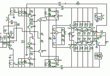
On a symasym type amp , this would be a most valuable addition since it does not have a fixed , stable current source like the blameless. Here is a picture (#2)of the whole thing (quasi killer with the better "blameless") , I just showed the Vbe last time.
OS
Attachments
one of the first jobs I did when I read that section back in 2001 was to pick out the maximally flat "tops" of the 4 lower plots. 16r suits 8mA, 27r suits 5mA.just through a 10-16R resistor. The self example
He says the 10-20R resistor "offers first order cancellation of Vbias variations due to current changes".
Further calculation brought up 10r suits >=10mA and 30r suits 4mA.
It does look like the extra r is moving towards zero as the VAS bias is increased. But where?
Ostripper, if you're worried use a PNP Vbe multiplier and keep the cap connected between E and C. This will eliminate the 10R resistor from the signal path.
C85 reminds me of:
http://www.diyaudio.com/forums/solid-state/168554-based-hugh-deans-aksa-55-a-5.html#post2250485
- keantoken
C85 reminds me of:
http://www.diyaudio.com/forums/solid-state/168554-based-hugh-deans-aksa-55-a-5.html#post2250485
- keantoken
Ostripper, if you're worried use a PNP Vbe multiplier and keep the cap connected between E and C. This will eliminate the 10R resistor from the signal path.
C85 reminds me of:
http://www.diyaudio.com/forums/solid-state/168554-based-hugh-deans-aksa-55-a-5.html#post2250485
- keantoken
The 10R resistor in the signal path is of no concern , as mr. self said, it is a small local feedback to compensate for current variations. Also we have 100r base stoppers right after the VBE .... so does it matter?? In chapter 12 , he makes "fun" of his own CCS with its 2 diodes which is why he says to never omit the 10R resistor. I don't have these problems with my cap multipliers and 2 more advanced CCS's.
I also have that "magic" cap in your link on my Vbe base, it keeps the Xover point the same (.6ma variation) across the entire audio spectrum , even with the IRFP's.
OS
then the extra resistor is in the path to the lower driver.
Yes, but with a singleton VAS no drive comes from that side, it's just a CCS. Not that it matters considering the base stoppers as OS pointed out...
Ostripper, the 10R resistor provides feedforward compensation like in a feedforward regulator (if you don't know what that is, look it up, don't guess). However at AC C85 changes this. If you adjust the 10R for DC bias stability, then at AC it will overcompensate, wasting energy through C86 and decreasing AC impedance.
Using a PNP Vbe multiplier like I said would help because then no AC would need to come through the 10R resistor.
- keantoken
you even forced me to draw it out.Yes, but with a singleton VAS no drive comes from that side, it's just a CCS. Not that it matters considering the base stoppers as OS pointed out...
There are two audio signal outputs from the Vbe multiplier.
The upper feeds the upper driver.
The lower feeds the lower driver.
NPN multiplier has the extra resistor in the top feed.
PNP multiplier has the extra resistor in the lower feed.
Whether it's a CCS or a bootstrapped resistor does not affect the two audio feeds to the driver stage.
Replace the lower CCS transistor with a complementary VAS. It looks exactly the same if you travel from +ve rail to -ve rail.
- Status
- This old topic is closed. If you want to reopen this topic, contact a moderator using the "Report Post" button.
- Home
- Amplifiers
- Solid State
- The MONGREL (supersym II)