Cross modulation is when uncontrolled current flows through the output stage from rail to rail. It happens because the ON device switches OFF slower than the OFF device switches ON.
For a short period of time both devices are at least partially on. At low frequency this is hardly noticed. As frequency rises the cross modulation gets worse.
I can see that your 80kb/s sampling rate rolls off the measured distortion above 10kHz. But for that red trace the measured value keeps on rising. This suggests that the actual distortion is rising much more rapidly than the graph shows and that is what I'm enquiring about. Does the continued rise in the distortion above 10kHz indicate someone happening?
Cross modulation is when uncontrolled current flows through the output stage from rail to rail. It happens because the ON device switches OFF slower than the OFF device switches ON.
For a short period of time both devices are at least partially on. At low frequency this is hardly noticed. As frequency rises the cross modulation gets worse.
Does it occur at the bias point where upper and lower devices handle over the job?
cross modulation or something else
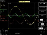
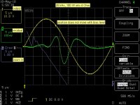
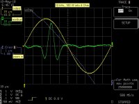
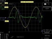
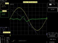
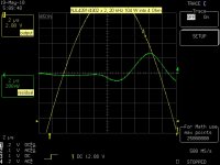
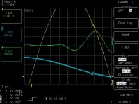
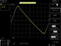
I take more measurements for the above issue - raising distortion at high freq. Hope these data can help one to interpret what is happening. Something is found from the output waveform when no speed cap installed.
Starting from the left figure:
20 kHz 50 W into 8 Ohm --- third harmonic dominates the distortion residual
20 kHz 100 W into 4 Ohm -- something (call it glitch) occurs on positive cycle
10 kHz 100 W into 4 Ohm -- glitch is not clearly seen in output
15 kHz 100 W into 4 Ohm: -- glitch is clearly seen in the positive cycle
The output load is a resistive load. The voltage and current waveform are inphase. The glitch does not seem to happen at voltage or current zero-crossing.
The right most figure is 20 kHz 100 W into 4 Ohm with speed-up cap installed. The glitch is hardly seen from the output waveform. It can be seen from the zoom in and distortion residual.
Attachments
-
 49811 two pair THD+N residual 20k 50w 8ohm.JPG133.1 KB · Views: 827
 -
 49811 two pair THD+N residual 20k 100w 4ohm B.JPG138.9 KB · Views: 794
 -
 49811 two pair THD+N residual 10k 100w 4ohm.JPG121.2 KB · Views: 772
 -
 49811 two pair THD+N residual 15k 100w 4ohm.JPG126.9 KB · Views: 747
 -
 49811 two pair THD+N residual 20k 100w 4ohm with cap.JPG118.4 KB · Views: 730
glitch
Hi Panson,
I'm no expert on these things, but, when I've seen this type of glitch in this location on the wave form, it's when looking at power supplys from diode ringing when charging the output caps.
Ken
The output load is a resistive load. The voltage and current waveform are inphase. The glitch does not seem to happen at voltage or current zero-crossing.
The right most figure is 20 kHz 100 W into 4 Ohm with speed-up cap installed. The glitch is hardly seen from the output waveform. It can be seen from the zoom in and distortion residual.
Hi Panson,
I'm no expert on these things, but, when I've seen this type of glitch in this location on the wave form, it's when looking at power supplys from diode ringing when charging the output caps.
Ken
Hi Panson,
I'm no expert on these things, but, when I've seen this type of glitch in this location on the wave form, it's when looking at power supplys from diode ringing when charging the output caps.
Ken
Hi Ken,
Thanks for you suggestion. I also looked into this possible cause by adding snubber cap 0.1 uF across all Sanken FMDG26S rectifier diodes. The glitch still exists after this mods. It seems the glitch taking a long time to settle with the caps added. Probably need to try value or RC snubber.
A load test using an 8 Ohm resistor connected to the supply rail +/- 40 V does not show any glitch in the ripple. Dynamic should be more useful. But I don't have an electronic load.
Left: no snubber
Middle: with snubber
Right: supply load test
Panson
Attachments
Last edited:
Those are they same kind glitches that raised havoc in my transformer tests here http://www.diyaudio.com/forums/planars-exotics/161485-step-up-transformer-design-4.html#post2137648 and here http://www.diyaudio.com/forums/planars-exotics/161485-step-up-transformer-design-3.html#post2133865 , I believe them to be crossover distortion and they got worse as load impedence got lower.
In those tests, my load impedence's were as low as an .5 ohm and lower as the frequency went up and it was a purely reactive load too boot, demanding much much more current than the amp could even dream of producing.
Just my thoughts. jer
In those tests, my load impedence's were as low as an .5 ohm and lower as the frequency went up and it was a purely reactive load too boot, demanding much much more current than the amp could even dream of producing.
Just my thoughts. jer
Hi Ken,
Thanks for you suggestion. I also looked into this possible cause by adding snubber cap 0.1 uF across all Sanken FMDG26S rectifier diodes. The glitch still exists after this mods. It seems the glitch taking a long time to settle with the caps added. Probably need to try value or RC snubber.
A load test using an 8 Ohm resistor connected to the supply rail +/- 40 V does not show any glitch in the ripple. Dynamic should be more useful. But I don't have an electronic load.
Left: no snubber
Middle: with snubber
Right: supply load test
Panson
Hi Panson,
RC filtering might remove it, also, you might try adding more capacitance near the output transistors say 1000uf each. I am going to try attaching a pdf written by Jim Hagerman, Hagerman Technologies on calculating optimum snubbers. To big to post... here is the link to his tech articles, scroll down and look for title "calculating optimum snubbers". Thanks to Jack Walton for the link
") .
. Ken
Ken
Hi Panson,
RC filtering might remove it, also, you might try adding more capacitance near the output transistors say 1000uf each.
Ken
Hi Ken,
I wonder electrolytic cap can handle such high freq glitch effectively. Film cap should be the choice.
Panson
Those are they same kind glitches that raised havoc in my transformer tests here http://www.diyaudio.com/forums/planars-exotics/161485-step-up-transformer-design-4.html#post2137648 and here http://www.diyaudio.com/forums/planars-exotics/161485-step-up-transformer-design-3.html#post2133865 , I believe them to be crossover distortion and they got worse as load impedence got lower.
In those tests, my load impedence's were as low as an .5 ohm and lower as the frequency went up and it was a purely reactive load too boot, demanding much much more current than the amp could even dream of producing.
Just my thoughts. jer
Thanks for your sharing. What amp do you use to driver the speaker?
hi Panson,
First of all ... need to mention that I'm not an expert !
I built an amplifier based on the LME49830+IRFP (So totally different from your setting), and I've face an issue (not sure it the same that you call "glitch"). I've done many measurements you can see few of them here : Projet : Ampli à base de LME49830 - "Gran Torino 150" - Page 29 - Amplification
My issue appears on SINUS and also on Square waves.
I don't know what is the exact topology of your amplifier ... but my issue was just that the resistor gate was too small.
Obviously the solution I found cannot be applied in your case, but if something simillar can be applied to your design.
COuld this come from the Ccomp ? Or any other element that may change the driving speed of the bjt ?
Brgds - Gilles.
hi Panson,
First of all ... need to mention that I'm not an expert !
I built an amplifier based on the LME49830+IRFP (So totally different from your setting), and I've face an issue (not sure it the same that you call "glitch"). I've done many measurements you can see few of them here : Projet : Ampli à base de LME49830 - "Gran Torino 150" - Page 29 - Amplification
My issue appears on SINUS and also on Square waves.
I don't know what is the exact topology of your amplifier ... but my issue was just that the resistor gate was too small.
Obviously the solution I found cannot be applied in your case, but if something simillar can be applied to your design.
COuld this come from the Ccomp ? Or any other element that may change the driving speed of the bjt ?
Brgds - Gilles.
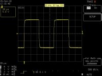
Hi Gilles,
Red curve input signal, blue curve output signal?
did you solve the problem by using larger gate resistors?
Panson
Yes ... Panson,
Red curve = INPUT (before pot)- Scale 1V/div
Blue curve = OUTPUT AMP - Sacle 10V/div or 20V/div
You can read the scale at the top left for Voltage, and on the TOP right for "Time"
My issue was solved using smaller Rgates.
We could think ... Smaller Rgate will increase instability due to the Frequency cut increase (Ciss).... But in fact if the value is TOO BIG that makes an issue too, as well as if the value is too small.
Originally, the Rgates were 220Ohms, and now, I've 150 Ohms, but thinking decrease the value down to 120, to see if it can improve what I've seen on capacitive load
The issue of the gate resistor has been raised in the National semicondiutor document : http://www.national.com/an/AN/AN-1645.pdf (page 10).
I'm still in the measuring process.
Hope this will help.
Best regards gilles.
LME49811 with CFP output
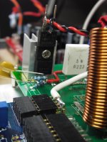
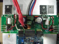
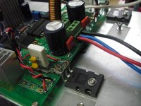
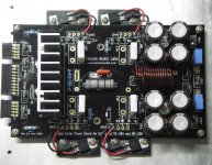
I modified the output power board to accommodate a CFP output stage. It consists on MJE15034/35 and MJL21194/93. The driver collector resistor is initially 120 R. Re is 0.22 R. Base stopper for driver is 100 R. The stopper very important here to avoid oscillation. The comp cap is 32 pF. Bias is simply generated by two diode and a trim pot. Each diode is attached to the driver heatsink as shown in the picture. Output coil and damping is employed.
Compared to emitter follower output stage, CFP is relatively less friendly. This is my impression at the moment.
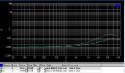
THD+N vs freq (BW=80k) for 18W/8R and 36W/4R is shown in the picture.
.
I modified the output power board to accommodate a CFP output stage. It consists on MJE15034/35 and MJL21194/93. The driver collector resistor is initially 120 R. Re is 0.22 R. Base stopper for driver is 100 R. The stopper very important here to avoid oscillation. The comp cap is 32 pF. Bias is simply generated by two diode and a trim pot. Each diode is attached to the driver heatsink as shown in the picture. Output coil and damping is employed.
Compared to emitter follower output stage, CFP is relatively less friendly. This is my impression at the moment.
THD+N vs freq (BW=80k) for 18W/8R and 36W/4R is shown in the picture.
.
Attachments
New layout for Initial Power Board
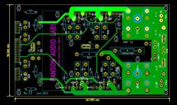
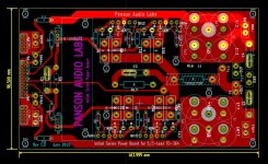
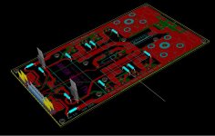
Here is a new power board for the Initial Series. The board accommodates two-pair 3-lead and 5-lead TO-264. Output coil and Zobel network are added. It will be released to PCB house soon. Comments are welcome.
Green: Bottom layer
Red: Top layer
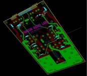
The 3D is not perfect since I have not build the 3D models for my component library.
Here is a new power board for the Initial Series. The board accommodates two-pair 3-lead and 5-lead TO-264. Output coil and Zobel network are added. It will be released to PCB house soon. Comments are welcome.
Green: Bottom layer
Red: Top layer
The 3D is not perfect since I have not build the 3D models for my component library.
Attachments
Last edited:
- Status
- This old topic is closed. If you want to reopen this topic, contact a moderator using the "Report Post" button.
- Home
- Amplifiers
- Chip Amps
- Comparing LME49810, 49830 and 49811