Oooops! I forgot to remark something about the schematic.
When doing my first tests, I found that, altougth the output of the MAX038 was a perfect square wave, it gets slightly distorted after being amplificated. When I disconnected the output of the opamp U4B from the input of the comparator U5A, it improved, and also when I reduced both the input and feedback resistors, R18 and R10. (they were originally 10K and 22K). What can the cause be? The bandwidth and slew rate of the amplifier seem far higher than needed, aren't they?
Best regards.
Hi Sergio
Just try to imagine how much (parasitic) capacitance it takes to form a 100 kHz (or whatever) lowpass with a 22 k resistor !
Whatever you do you have to be always aware that you are building a precision RF circuit used to process audio !
Something that hasn't been discussed so far are the freewheeling diodes that handle the "backward" current caused by the output inductor. Depending on switching frequency you can't always rely on the built in diodes of the mosfets.
Regards
Charles
Thanks for your fast response time, Charles. ")
So, if I have understood, the high previous value of 22K in the feedback of the U4B amplifier in conjunction with the parasitic capacitance of the comparator can distort the signal, is that the problem? I reduced it to 2k2 and it improved, but is not by far as perfect as the MAX038 output. Any sugestions?
Best regards
Hi Sergio
I was just talking about a possible cause. Be aware that the dv/dt of a triangular may not look very high but it is still a demanding signal.
To avoid unnecessary distortion an opamp must be faster by at least an order of magnitude. The gain-bandwidth product has to be quite high as well: Just try to imagine how much NFB is left at the fundamental frequency of the triangular, let alone it's harmonics !
And don't forget that the lower and upper edge of the triangular represent a very high slew-rate signal.
I forgot to look at your circuit again before starting to post but I will have another look to see, why you use this opamp at all.
Regards
Charles
Hi Sergio
I assume it is there only to increase the amplitude of the triangular by a factor of two.
While a large triangular amplitude is a good thing, regarding susceptibility of the modulator to spikes etc, it's linearity is important as well.
So I would suggest to try it with and without this opamp stage and compare the results (the feedback has to be dimensioned accordingly).
Regards
Charles

Thanks, Charles.
Of course, this stage was designed to increase the amplitude of the triangle only, but given its distortion, perhaps it is better to leave it as is. (2Vpp).
Yes, the design is done in Protel. If you don't mind, I will wait until the PCB is completed and the board relatively tested before publishing all, although if you really want them I can post them.
I really like this way of work. I feel very supported. Thanks!
to phase,
yes, damping works also with no load at all and yes it only damps filter resonance. But it makes it easier to close the output loop around filter.
to ssanmor,
I see you will be running your amp open loop. Then modulator and drive circuits timing errors will be main sources of distortion. I agree with phase you would need at least 50-100 MHz GBW opamp for triangle amplification. One alternative is LM359 norton amp which produces really nice triangle. If you stay with 2V output from MAX, i recommend you change comparator U5A to something faster. I had good results with LT1394 from Linear Technology. I also suggest you tie pin 2 of U2 directly to the source of Q3 and have separate supply capacitors for VDD and VCC of U2 with VDD connected directly to VDRIVER and put 2.2 Ohm resistor between VDD and VCC.
regards, Jaka Racman
I see you will be running your amp open loop
Sorry i did not look at the upper left corner of your schematic. Have you done simulation of closed loop response? I have a strong feeling that your amp will oscillate.
Regards, Jaka

Hi Sergio
I didn't do any calculations but my feelings tell me that Jaka is right. With this circuit you shouldn't take feedback from the output filter, the phase-margin wouldn't be sufficient.
I would take it from the input of the filter for a first attempt. You need topologies that are a little more complicated than dominant-pole compensation in order to be able to take feedback from the output of the filter. You might even have to recalculate RA1 and C23.
If you have it up and running I could point you to a trick that is related to the one mentioned above by Jaka for taking feedback from the filter output. I haven't used it in practice so far (i.e. only for simulations) but it should work according to my imagination.
Regards
Charles
Ah, Ok.
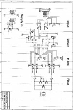
I think that, as I haven't posted the root sheet of the schematic, there has been a little confusion: my schematic takes the feedback from the input of the output filter, but I understand that the names of the ports are confusing.
However, when it is up and running, as Charles says, my idea is to try to take the feedback from the very output. Your help will be very useful here!
Thanks and sorry for the confusing schematics.
- Status
- This old topic is closed. If you want to reopen this topic, contact a moderator using the "Report Post" button.
- Home
- Amplifiers
- Class D
- My very first Class D pwm (switching) amplifier.