Dear Ken,
Here the schematic attached.
I got you about the NLJ3281D. You took the worst case scenario with -25 degrees celsius which indeed gives an hFE of about 85.
One reason to go with multiple drivers is to give the system more current headroom, but most important, the distortion of the LME49811 rise excessive above 1,2mA remember measurements from Panson.
With kind regards,
Bas
Bas,
I'll have to think about this a bit, but, my first reaction is that the drivers are in parallel not series, so, your driver+ouput hFe is not increased, so the damands on the LME49811 are the same. For example, when you look at a darlington transistor it will have a hFe of 5000 to 20,000 - that number is arrived at by multiplying the driver hFe x the output hFe, so in the example above your darlington configuration would be 200 x 85 =17,000hFe. But, you don't multiply the 17,000 x 3 because you have 3 pairs... it's still 17,000. If you want to reduce the load on the LME49811, you would need to add pre drivers and as I've said in this thread, I think that overkill - Andrew probably will disagree. Multiple drivers in parallel doesn't reduce the load on the LME49811. The math using the 17,000hFe is 21A/17,000hFe = 1.2ma same value as the prior equations going transistor by transistor.
I guess you could try your layout. But, the variations in hFe for the darlingtons will probably be more extreme than between just the outputs transistors alone. So, the current sharing might not be as good. The 10 ohm resistors will need to be increased - to what value I don't know.
Hope this helps.
Ken
Dear Ken,
You are right. I do the math over and over again and one way or another I also come with the same 1,2mA for the driver.
Thanks for the insight. I was confused before, but now not anymore. In that case I should go with one driver instead.
With kind regards,
Bas
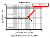
I don't know what data or graphs you two are using.
NJL3281 is specified at gain 75 @ 5A @ and at 45 @ 8A both at 25degC.
The graph of typical gain @ 7A is ~80 at 25degC.
I think from this evidence you should use somewhere between 50 & 60 for the gain at 7A.
3Pair of NJL each passing 7A, 21Atotal, requires ~21/55 ~=382mA of total base current. A single driver will pass all this as emitter current.
In the previous example for 4A of output current from each device the base current is 200mA using the gain of 20 as specified.
4pair will require 800mA of base current for a total of 16A of output current.
If the driver has a gain of 50 @ 800mA then the driver base current will be 16mA. i.e 16A @ output requires 16mA from the VAS or pre-driver if used.
Look at the device gains, 20 & 50. multiplied that comes to 1000, yes, 1mA becomes 1A if the gains do not vary with current passed, i.e. linear BJTs.
I don't know what data or graphs you two are using.
NJL3281 is specified at gain 75 @ 5A @ and at 45 @ 8A both at 25degC.
The graph of typical gain @ 7A is ~80 at 25degC.
I think from this evidence you should use somewhere between 50 & 60 for the gain at 7A.
3Pair of NJL each passing 7A, 21Atotal, requires ~21/55 ~=382mA of total base current. A single driver will pass all this as emitter current.
In the previous example for 4A of output current from each device the base current is 200mA using the gain of 20 as specified.
4pair will require 800mA of base current for a total of 16A of output current.
If the driver has a gain of 50 @ 800mA then the driver base current will be 16mA. i.e 16A @ output requires 16mA from the VAS or pre-driver if used.
Look at the device gains, 20 & 50. multiplied that comes to 1000, yes, 1mA becomes 1A if the gains do not vary with current passed, i.e. linear BJTs.
Thanks Andrew for your comments.
In your example for 21Apk the LME49811 driver must deliver 1,9mA if I use the 2SC6072/2SA2190 drivers with hFE 200 at 250mA. I still think this is reasonable. Since my design is a bridged design, the total current able to being delivered to the speaker should then be 42Apk. Even if the driver/outputstage is ready to deliver that, I wonder what kind of power-supply will keep this up.
I will work on a new schematic, and post it here and take all the advice given by you and Ken with me. I'll be back soon
")
Have a nice weekend.
With kind regards
Bas
Last edited:
Dear,
Going back again to my previous post.
Looking at Panson's measurements it seems that 1,9mA for the LME49811 is to much for a low distortion performance... dilemma dilemma..
http://www.diyaudio.com/forums/chip-amps/143163-comparing-lme49810-49830-49811-a-2.html#post1818115
I want so desperately omit the 3rd driver stage and stick to a two stage EF. But seems hard to accomplish.
With kind regards,
Bas
Dear,
Going back again to my previous post.
Looking at Panson's measurements it seems that 1,9mA for the LME49811 is to much for a low distortion performance... dilemma dilemma..
http://www.diyaudio.com/forums/chip-amps/143163-comparing-lme49810-49830-49811-a-2.html#post1818115
I want so desperately omit the 3rd driver stage and stick to a two stage EF. But seems hard to accomplish.
With kind regards,
Bas
Bas,
Audioman54 has built a LME49811 100w amp with darlington output and no predrivers. I can't remember the exact thd he cited, but I seem to recall that it was below .001%.
I also noticed that you're planning on a bridging typology, is that to keep the drive current low? Seems like overkill to me.
I haven't preformed a full power test yet. But just recorded .0024% Thd with my LME49811 driving my Allison output stage - no predrivers and 15032/33 as the drive transistors.
Ken
Bas,
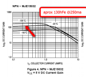
I thought I might do the math again with the MJE15032/33's and the NJL3281
NJL 3281 hFe at 7A approx 105
MJE15032 hFe at 250ma approx 130
105hFe x 130hFe = 13,650
21A/13,650 = 1.5ma
I have also found that hFe rises with voltage both of these hFe's were measured at 5v.
I've seen your other thread on this design and now think overkill is good.
One other bit, you gain setting resistors are 1k/20k ? you need a gain of at least 26 or the amp may be unstable - national app notes -
Ken
Bas,
I thought I might do the math again with the MJE15032/33's and the NJL3281
NJL 3281 hFe at 7A approx 105
MJE15032 hFe at 250ma approx 130
105hFe x 130hFe = 13,650
21A/13,650 = 1.5ma
I have also found that hFe rises with voltage both of these hFe's were measured at 5v.
I've seen your other thread on this design and now think overkill is good.
One other bit, you gain setting resistors are 1k/20k ? you need a gain of at least 26 or the amp may be unstable - national app notes -
Ken
I had wanted to put in some images...
Attachments
Bas,
I thought I might do the math again with the MJE15032/33's and the NJL3281
NJL 3281 hFe at 7A approx 105
MJE15032 hFe at 250ma approx 130
105hFe x 130hFe = 13,650
21A/13,650 = 1.5ma
I have also found that hFe rises with voltage both of these hFe's were measured at 5v.
I've seen your other thread on this design and now think overkill is good.
One other bit, you gain setting resistors are 1k/20k ? you need a gain of at least 26 or the amp may be unstable - national app notes -
Ken
Dear Ken,
Today I did some measurements as well with different loads on the LME49811.
In general you want to relieve the VAS from any load. Unfortunately the MJE15032/33's have a relative high Cop, which the LME49811 dislikes.
The LME49811 do start to rise in THD with more then 1.2mA by 37 volt in my measurements. In this setup I use a 30 Ohm resistor as load, together with 47pF capacitance. It was clearly that the LME49811 doesn't like capacitive load and distortion rise with higher capacitance. That is why I consider a 3 stage EF to "unload" the LME49811. I will post my new schematic later today.
The reality is off course, that we talking about "worse case" scenario's all the time, and with such a high current delivery our speakers will distort much more already then the LME49811. But it just feels better if you can stay far away from higher THD levels or headroom issues.
One more note. You are right about the gain setting. My mistake! I only worked with the LME49810 before and there the minimal gain limit is 10 for this IC. Without thinking I assumed the same is truth for the LME49811, but I was wrong. I should read my data sheets more careful
It is a bit of a problem this gain of 26, because in my bridged design this result in a gain of 52 which is to much.
I do love bridged designs because of the double slew-rate, the suppression of odd harmonics and the iron grip on the speaker (even though damping factor will get twice as less).
Another reason is, that in my experience, amplifier designs tend to sound better with lower PSU voltages. This is possible with a bridged design while still maintain high output power. (hence twice as much current per amplifier halve).
With kind regards,
Bas
Are you shure you can design a pre-driver better than the one included in the LME49810 [snip]
That's a valid question. I don't see any big reason to use a 811 alongside the 810 or 830.
That's a valid question. I don't see any big reason to use a 811 alongside the 810 or 830.
Indeed a very good point. One of the first reasons to stick with a chip VAS is because I can't design a VAS as good and accurate then an LME chip is.
I never built an amplifier with the LME49811 yet, only with the LME49810, and the sound result where nothing more then sublime. But then, Audioman54 put me on think, and the idea the output stage in the LME49810 is continue in class B bothers me a bit.
With kind regards,
Bas
Last edited:
Dear Ken,
Today I did some measurements as well with different loads on the LME49811.
In general you want to relieve the VAS from any load. Unfortunately the MJE15032/33's have a relative high Cop, which the LME49811 dislikes.
The LME49811 do start to rise in THD with more then 1.2mA by 37 volt in my measurements. In this setup I use a 30 Ohm resistor as load, together with 47pF capacitance. It was clearly that the LME49811 doesn't like capacitive load and distortion rise with higher capacitance. That is why I consider a 3 stage EF to "unload" the LME49811. I will post my new schematic later today.
The reality is off course, that we talking about "worse case" scenario's all the time, and with such a high current delivery our speakers will distort much more already then the LME49811. But it just feels better if you can stay far away from higher THD levels or headroom issues.
One more note. You are right about the gain setting. My mistake! I only worked with the LME49810 before and there the minimal gain limit is 10 for this IC. Without thinking I assumed the same is truth for the LME49811, but I was wrong. I should read my data sheets more careful
It is a bit of a problem this gain of 26, because in my bridged design this result in a gain of 52 which is to much.
I do love bridged designs because of the double slew-rate, the suppression of odd harmonics and the iron grip on the speaker (even though damping factor will get twice as less).
Another reason is, that in my experience, amplifier designs tend to sound better with lower PSU voltages. This is possible with a bridged design while still maintain high output power. (hence twice as much current per amplifier halve).
With kind regards,
Bas
Bas
The 15032/33's do seem like a bit of overkill, but, I've found them to be robust and stable.
Have you been able to get the amp to run with the Toshibas you mentioned? As I mentioned, I've had zero success with 2sc4793 / 2sa1837. The models work in my sim, but, not in real life. I'll be interested to hear.
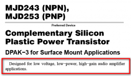
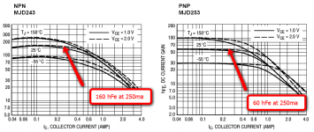
The other driver I've used with some success is the MJD243/253. They might be good for your application - look at the description I've highlighted. 50pf Cob. But the PNP has a pretty low hFe.
Ken
Attachments
Bas
The 15032/33's do seem like a bit of overkill, but, I've found them to be robust and stable.
Have you been able to get the amp to run with the Toshibas you mentioned? As I mentioned, I've had zero success with 2sc4793 / 2sa1837. The models work in my sim, but, not in real life. I'll be interested to hear.
The other driver I've used with some success is the MJD243/253. They might be good for your application - look at the description I've highlighted. 50pf Cob. But the PNP has a pretty low hFe.
Ken
Dear Ken,
No I have a hard time to obtain the Toshiba's here in the Netherlands.
In which way you didn't got them to run? They didn't conduct? Oscillations?
They are designed for home theatre receivers. I am kind of stubborn
and I think I can't give up before I have them working With kind regards,
Bas
That's a valid question. I don't see any big reason to use a 811 alongside the 810 or 830.
http://www.diyaudio.com/forums/solid-state/132471-national-opamp-inflation-2.html#post1707365
and
http://www.diyaudio.com/forums/solid-state/132471-national-opamp-inflation-3.html#post1708866
With kind regards,
Bas
Audioman54 put me on think, and the idea the output stage in the LME49810 is continue in class B bothers me a bit.
With kind regards,
Bas
Pavel Macura chooses here a class B driver and he explains the reasons.
http://www.diyaudio.com/forums/soli...olid-state-power-amplifier-2.html#post1993755
Pavel Macura chooses here a class B driver and he explains the reasons.
http://www.diyaudio.com/forums/soli...olid-state-power-amplifier-2.html#post1993755
Dear bobodioulasso,
I finished reading it. As far as I understood, he doesn't bias the driver stage in class B but he use the self type 1 EF with the emitter resistors tied to the output. This would slightly worser switch off behavior (according to Self) but doesn't say it is in class B. It depends how much Idle current you let run through the drivers.
With kind regards,
Bas
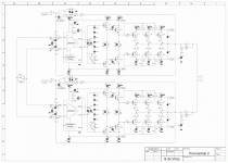
Dear,
Here the schematics of my new plan. However lot of things have to be figured out.
First a resume.
I decide to not give up on the toshiba driver transistors and make it as my goal to make them work That said this is the planned configuration. Note the hFE's are chosen for worse case scenario's and will be higher in real life situations.
First driver: 2SC3423/2SA1360 (hFE +/-100)
Second driver: 2SC6072/2SA2190 (hFE +/- 180)
Power stage:NJL3281D/NJL1302D (hFE +/- 70)
Once again the math in this new situation. The end goal is to reach 21Apk
21Apk/70=0,3A
0,3A/180=1,67mA
1,6mA/100=0,0167mA
The LME driver will see hardly any load and will have the lowest THD in this configuration. However on the prototype boards, I will listen and measure with as well the first driver omitted as activated. This would be the only way to find out if we really need them or not.
I do have a big gain problem in this configuration. The first limitation is that the LME49811 may not work with gain below 26 (in my schematic I am already below). Since I drive both chips balanced each amplifier half will have double the gain. Once bridged both amplifiers the gain doubles again! as result I will end up in a way to high total sensitivity and gain.
Driven by a balanced +/- 1volt signal I will have an amplifier gain of 80 equal to 32dB. If I change both amplifier gains of 26, I will end up in a total gain of 104!
Either I need to reduce the input signal passive, or limit the open loop bandwidth in the feedback loop to be able to use the chips with lower gain settings.
Makes it more attractive to go for the LME49810 instead, since that chip may be used with gains start at 10.
One more question. To make sure the driver stage is always in class A I assume the Idle current should be as high as the maximum to be expected to deliver current. I am correct in this?
That would be 1,67mA idle current for the first driver stage and 300mA for the second driver stage.
With kind regards,
Bas
Here the schematics of my new plan. However lot of things have to be figured out.
First a resume.
I decide to not give up on the toshiba driver transistors and make it as my goal to make them work
That said this is the planned configuration. Note the hFE's are chosen for worse case scenario's and will be higher in real life situations.First driver: 2SC3423/2SA1360 (hFE +/-100)
Second driver: 2SC6072/2SA2190 (hFE +/- 180)
Power stage:NJL3281D/NJL1302D (hFE +/- 70)
Once again the math in this new situation. The end goal is to reach 21Apk
21Apk/70=0,3A
0,3A/180=1,67mA
1,6mA/100=0,0167mA
The LME driver will see hardly any load and will have the lowest THD in this configuration. However on the prototype boards, I will listen and measure with as well the first driver omitted as activated. This would be the only way to find out if we really need them or not.
I do have a big gain problem in this configuration. The first limitation is that the LME49811 may not work with gain below 26 (in my schematic I am already below). Since I drive both chips balanced each amplifier half will have double the gain. Once bridged both amplifiers the gain doubles again! as result I will end up in a way to high total sensitivity and gain.
Driven by a balanced +/- 1volt signal I will have an amplifier gain of 80 equal to 32dB. If I change both amplifier gains of 26, I will end up in a total gain of 104!
Either I need to reduce the input signal passive, or limit the open loop bandwidth in the feedback loop to be able to use the chips with lower gain settings.
Makes it more attractive to go for the LME49810 instead, since that chip may be used with gains start at 10.
One more question. To make sure the driver stage is always in class A I assume the Idle current should be as high as the maximum to be expected to deliver current. I am correct in this?
That would be 1,67mA idle current for the first driver stage and 300mA for the second driver stage.
With kind regards,
Bas
Attachments
Last edited:
We are not far from the Rotel O.S.values...
Did you intentionally ommit the source to sink resistors?
I have read somewhere -do not recall where- D3,D4... aren't necessary with LME...
I should have said classAB.
The way he does is AB, don't you think?
When Audioman says class B about the 49810 last stage, i think he means AB too...
Did you intentionally ommit the source to sink resistors?
I have read somewhere -do not recall where- D3,D4... aren't necessary with LME...
I finished reading it. As far as I understood, he doesn't bias the driver stage in class B but he use the self type 1 EF with the emitter resistors tied to the output. This would slightly worser switch off behavior (according to Self) but doesn't say it is in class B. It depends how much Idle current you let run through the drivers.
I should have said classAB.
The way he does is AB, don't you think?
When Audioman says class B about the 49810 last stage, i think he means AB too...
Last edited:
We are not far from the Rotel O.S.values...
Did you intentionally ommit the source to sink resistors?
I have read somewhere -do not recall where- D3,D4... aren't necessary with LME...
I should have said classAB.
The way he does is AB, don't you think?
When Audioman says class B about the 49810 last stage, i think he means AB too...
Dear bobodioulasso,
I would rather also omit D3, D4 and D8, D9 since they have leakage. But I am bit afraid for what will happened if the cones give heavy EMK.
Since the capacitance of the 2SC3423/2SA1360 drivers is so low, and since the LME chip at worse case only need to deliver 0,0167mA I decided not to put resistors in serials with the source and sink pins since I think the LME hardly sees any load anymore. Less is more.
I would be interesting to know what the idle current biassing is of the driver stage inside the LME49810, but I guess we never know. In my design I want to make sure the driver stage is always in class A. As a matter of fact, I consider to invest in heavy heat sinks and power supply, add some extra pairs of output devices and bias the whole amplifier the first 20 or 25 watt in class A.
With kind regards,
Bas
- Status
- This old topic is closed. If you want to reopen this topic, contact a moderator using the "Report Post" button.
- Home
- Amplifiers
- Chip Amps
- LME49810/STD03 parallel pairs