Here again Bas Horneman homepage for the complete documentation: http://basenjes.de/tubes/data/sb/ShuntRegManual_With_SB Notes.pdf
Cocolino, there is no PCB at the moment, by I'm putting together an other small PCB order. Please send me a private email to bergeron.syl@videotron.qc.ca with your full name, shipping address, private email to reach you and the qty of PCB you want. I may order the PCB by next week.
FET update. Just paid the FET to Walter, there are leaving Finland tomorrow. Current price (without any possible custom charges at my end) is 1.25U$ each.
As soon as I get them, I'll send you an email with the final shipping cost and the FET amount that your ordered.
Thanks...
SB
FET update. Just paid the FET to Walter, there are leaving Finland tomorrow. Current price (without any possible custom charges at my end) is 1.25U$ each.
As soon as I get them, I'll send you an email with the final shipping cost and the FET amount that your ordered.
Thanks...
SB
Check the FET tracking. They left Finland 21 Nov at 4:50. I would expect them to show to my door this week.
Small suppl. PCB Order. I have enough buyers to place a very last small batch order.
Please check you email box for payment messages. Thanks...
NOTE: I ordered a few extra, and I can always have people that back out of the deal. So if you want some send me an email, we never know, I may be able to get your order...
Last edited:
FET Update. I received the post office notification today. The FET should be there tomorrow. I'll try to get some kit out the door as soon as Saturday. Check your email.
Second small GB: Still some PCB available. They will be the last ones for sure. Send me an email if interested.
Second small GB: Still some PCB available. They will be the last ones for sure. Send me an email if interested.
FET Info.
The FET are coming from an official Toshiba distributor and should be the real thing. I plan to test a few samples before packing them.
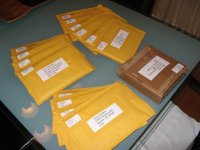
All FET will be handle over a static free station, with grounded wrist strap, and packed into 3M Static discharge bags.
HOWEVER, I'm not a part distributor, or reseller So there is no other warranty that the FET are real Toshiba part and suppose to be all good. I won't test all of them that is sure! So, if you get some defective part at your end, then I'm not responsible...Hope you understand my point. It will be enough work like it is to count all these small parts, packed them, etc...
Bye.
The FET are coming from an official Toshiba distributor and should be the real thing. I plan to test a few samples before packing them.
All FET will be handle over a static free station, with grounded wrist strap, and packed into 3M Static discharge bags.
HOWEVER, I'm not a part distributor, or reseller
So there is no other warranty that the FET are real Toshiba part and suppose to be all good. I won't test all of them that is sure! So, if you get some defective part at your end, then I'm not responsible...Hope you understand my point. It will be enough work like it is to count all these small parts, packed them, etc...Bye.
Got the FET  . Bad news is I got charge again with custom fees
  . Final price for each FET is 1.42$ each. Sorry guys, c'est la vie. By their look, they are real , an other good news, in the days of counterfeit parts. I'll test some tomorrow, and start packing all these little guys.
I'll get back to each of you with the final payment, including the FET and shipping cost.
Thanks...
. Bad news is I got charge again with custom fees . Final price for each FET is 1.42$ each. Sorry guys, c'est la vie. By their look, they are real , an other good news, in the days of counterfeit parts. I'll test some tomorrow, and start packing all these little guys.I'll get back to each of you with the final payment, including the FET and shipping cost.
Thanks...
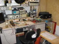
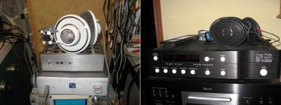
While I`m doing so, I have some nice Scotch (Glenmorangie, special edition) and I`m listening to some nice music using my late night setup: new AKG K-701, PS Audio GSHA haeadphone amp, Ack!DAC and ML37 Transport. Present CD, StockFish Records Sampler Volume 2, a killer recording and just handsome music.
Attachments
Here again Bas Horneman homepage for the complete documentation: http://basenjes.de/tubes/data/sb/ShuntRegManual_With_SB Notes.pdf
Hi, I am assembling one of these boards and noticed that the electrolytic caps (except C10) are shown with the (+) sign in wrong way on the parts placement diagram. I don't know if this has been brought up before.
Daniel
Last edited:
Hi, I am assembling one of these boards and noticed that the electrolytic caps (except C10) are shown with the (+) sign in wrong way on the parts placement diagram. I don't know if this has been brought up before.
Daniel
I haven't seen it brought up before. And you are correct. I'm mystified where that parts placement diagram comes from. It's not the one I have in my possession.
I'm busy assembling my third and fourth board. Boards one and two tested a-okay. Just follow the legend on the PCB. It's 100% correct.
One observation I would like to pass on is the matter of trimming R11 and R21 in the two 2SK369/170 constant current sources.
My advice would be to treat R11 (120R) and R21 (100R) as highly provisional. In other words, solder them in only part way.
In my experience thus far, these values are too high to get the two CCSs to pass, respectively, more than 2mA and more than 3mA.
In practice, I found I needed R11 to be 75R to get the T3-controlled CCS to pass >2mA, and for R21 to be 44.6R to get the T5-controlled CCS to pass >3mA.
As far as I know, and I built and tested 4 PCB myself, the PCB silkscreen is Ok, no error. The parts placement diagram is maybe from the original documentation from Emile. Here the original silkscreen from the PCB design software.
R11, R21 indeed depend on the FET IDGS current. Depending on the FET, you may need to trim these resistors to get the correct voltages. Check the schematic with notes, from the doc for the correct voltages.
This is even more important here for you guys since you have 2sk369BL and not V, these resistors will certainly need to be adjusted.
FET are all tested and are all Ok. Should be able to send a few kits tomorrow.
Attachments
R11, R21 indeed depend on the FET IDGS current.
Of course! Why didn't I think of that?
Gone for the rest of the week for work. I'm ready to ship some kit, but it has to wait until Saturday.
Last batch of PCB ordered. PCB plant close just before Christmas, Dec 19th. I hope to get the PCB by then.
David Husak you sent me an email, but I cannot reply to you. I got an error with your email address. Try to send me a private email on this forum, or give me an other address. Yes, I still have two PCB available for you. Thanks...
I am not able to get these geegaws to work. The voltage available at the non-inverting pin of the op-amp is too low. I measure 0.015V. It really should be something like 7V. It's not the voltage divider network, R18, R19, R3, R17, that is the problem. C2 and D3 are pulling the voltage down, apparently. Way down.
I've built four of these boards, and none of them work. The low voltage readings all checked out, the CCS is fine, the op-amps are fine, but the shunt reg proper doesn't work because the op-amp won't pass a signal to the gate of T4. Why should it? The voltage derived from the B+ is way lower than the reference voltage of, in my case, 6.9V.
Oh well.
First thing, the regulator doesn`t work without a load at its output. Try something as 22K at the output, this is the load I used to get the measurement values on the diagram. Be sure to use a resistor that can accept the dissipated power.
Don`t worry, this board had been assembled by countless user, and it had been checked. It is working. Since all four PCB got the same results, it is probably a systemic error (you did the same thing on all 4 PCB).
Try this. Don`t install the op-amp (U1), if installed on a socket, then measure Vout just after R3, it should change when you adjust R3, if not, D3 is probably installed in reverse. This is a simple voltage divider, and the op-amp input impedance is high, so it won`t load it. D3 is just a protection, and normally in normal operation (its Vzener is 9.1V) it shouldn`t be turn on. Worse can scenario it may be installed in reverse, shorthing the reference voltage.
Other thing to do, please write down on the included schematic, your own voltage readings, scan it and send it back to me.
- Status
- This old topic is closed. If you want to reopen this topic, contact a moderator using the "Report Post" button.
- Home
- Group Buys
- HV Shunt Regulator 2009 GB