and setting bias voltage too low results in even worse distortion.anatech said:Note that setting bias too high will always end up with higher distortion.
Hi Andrew,
The point? Find the proper bias level. I'm going to bet that it's a lower value than what you may expect. Even those sound card programs will allow you to find out where this level is. It's DIY all the way.")
-Chris
To be accurate, that is only a valid statement if you succeed in reducing the current in the output transistors to zero. In fact, the distortion does drop more quickly towards the optimal bias point than it does as you over bias. That doesn't really prove your statement to be accurate since what you will actually hear is only gross distortion. Slight under bias will not generate horrible amounts of terrible distortion. What you want is the proper bias either way.and setting bias voltage too low results in even worse distortion.
The point? Find the proper bias level. I'm going to bet that it's a lower value than what you may expect. Even those sound card programs will allow you to find out where this level is. It's DIY all the way.
-Chris
anatech said:Hi Steve,
That's not really a correct answer. I used MJW0281A and MJW0302A and ended up with around 20 mA bias I think. I posted the exact value in the original pages. Most manufacturers were running their outputs around 20 ~ 30 mA per device before the "hotter is better" silliness that became a long lasting fad.
Hi Chris,
As I had quoted MikeB's original design, I assumed his web original web site
[http://www.lf-pro.net/mbittner/Sym5_Webpage/symasym5_3.html] was one of the most authoritative sources. The trouble is there are now so many posts on this amplifier, with various tweaks, it's becoming time consuming reading all the relevant material.
Just to clarify, are you referring to AAK's version or the original for this level of bias?
Regards,
Steve
Hi All,
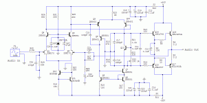
It's been a while but I'm glad to be back. I'm currently testing my new Symasym PCB (I know, long overdue) and I need some help on the design to make sure I'm not missing anything. Specifically I'm wondering if the bias circuit for Q3, and Q4 can be improved? Could it be the cause of a slight bit of hum that I hear with my ears right up to the woofer with the inputs grounded? My original PCB design is dead quiet.
I'll be posting some pictures of the assembled boards, and a pic of the PCB art work shortly. The board is the same size as the original (3" x 5") version
but with the added flexibility to easily configure the board to operate with different inputs and outputs devices. Here's the schematic.
Best Regards,
Al
Attachments
If there like me they probably have their boards laying around collecting dust. Good to here from you Ryssen.
BTW, that reminds me, I have four of my original boards unpopulated that I'm giving away for free. Just pay shipping. I also have two assembled prototype boards 100 watts per channel into 8 ohms on heatsinks that I'm selling for $25.00 each, that's $50.00 for both plus shipping.
BTW, that reminds me, I have four of my original boards unpopulated that I'm giving away for free. Just pay shipping. I also have two assembled prototype boards 100 watts per channel into 8 ohms on heatsinks that I'm selling for $25.00 each, that's $50.00 for both plus shipping.
Hi Andrew,
The new boards ground scheme is basically the same as the original. Plus, when I put a jumper across the emitter and collector of Q3 and Q4, disable the bias circuit, and replace the 2sk170's with 2n5551 it's dead quiet. So it appears to only happen when I'm using the Jfet inputs. That's why I think it may be the bias circuit ZD1,C26,C27, and R31.
The new boards ground scheme is basically the same as the original. Plus, when I put a jumper across the emitter and collector of Q3 and Q4, disable the bias circuit, and replace the 2sk170's with 2n5551 it's dead quiet. So it appears to only happen when I'm using the Jfet inputs. That's why I think it may be the bias circuit ZD1,C26,C27, and R31.
I built up 4 of the previous boards. Very pleased with them too. A pair of these boards forms my power amp in my main hifi setup, and has done for a while. So I'm keen to have a go at the next version.
I'm no designer but here's an idea.
Is there any value in having a separate regulated power supply for the front end? But keeping the power supply for the main drivers on board.
I'm no designer but here's an idea.
Is there any value in having a separate regulated power supply for the front end? But keeping the power supply for the main drivers on board.
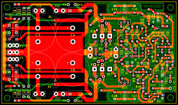
Is any of this "plane" connected to another part of the circuit?C24 and R29 connect to ground. The red trace is there to make sure that both pins are connected to ground on the top side of the board (green plane) if one of the through holes fails to connect. Probably not necessary, but it doesn't hurt just in case.
Could a hum voltage be imposed across your input circuit and create the noise you are hearing?
The green ground plane connects all the grounds in the amplifier section together and connects to the power supplies red ground plane found in the center of the board labeled GND. This is the star ground where the speaker's ground wire connects to.
It turns out that after looking into it some more last night the hum is only audible when the amp is first turned on but goes away once it warms up. So it shouldn't be a problem, but I will investigate it further and possibly try a different bias circuit for Q9 and Q10. Other than THD looks great, comparable to my original board and MikeB's design.
Thanks Andrew for looking into it.
Regards,
Al
Hi chalkandtalk,
I'm glad you liked the boards. I don't think that adding a seperate regulated PS would any value, plus I'd like to keep it simple. But I'm working on a external PS for those that would like to use a single transformer for two channels. I may also try just the amplifier without the PS on the same board. Since the amp alone measures 2.95" x 2.65" this may interest some. It would be no bigger than a chip amp but with better sound.
Regards,
Al
Hi all.
The PS on the amp board mean no harm only benefits I guess, since the transformer must be kept away? If you are not going to make two boxes - the amp and the PSU.
AAK is your PCB double-sided?
Besides, there is a reserve space to make traces more thicker for better audio performance and lower circuit impedance sake, if I'm not missing smth.
Do you know the shipping cost by post to Ukraine?
Regards.
Hi AndriyOL,
The PCB is double sided. The green layer is on the top side, red bottom. Signal traces are 52 mils which is more than enough. The power traces are 110 mils, they could made thicker but it should be Ok considering the trace length is 1.6".
Are you interested in the four unpopulated boards, or the assembled prototype boards with heat sinks?
Al
I think if impedance of routs is lower it's always better plus more reliable traces despite there is nothing to sacrifice instead.
I presume that green layer is a ground plane. Have you thought using single point ground system, adding snubbers to PSU? It may have far better performance results.
I can't find R3 on your PCB, likewise R5, R7 on the schematic.
I guess two 220uF as C18-21 will have worse ESR than one 1mF cap.
Maybe you should try to place output devices on the bottom side of the board, due to better heat distribution through whole heatsink, cause it always coming up. Otherwise bottom side will be cooler than upper side. From this point it would be better I think if output devices be placed in parallel at the bottom center of the heatsink and between each other.
I'm interested in your finest unpopulated four or maybe eight boards.
Regards,
Andriy.
the symasym PCB had all the returns (grounds) incorporated.
Where can I find the original symasym PCB design?
- Status
- This old topic is closed. If you want to reopen this topic, contact a moderator using the "Report Post" button.
- Home
- Amplifiers
- Solid State
- Symasym 5.3 "AAK model" builder's thread