Tube newbie question: I had this 5842 grounded grid circuit built from Yeo's diyparadise.com, what is the best way to bump the output a little bit?
Instead of the 120H choke, I used a 10K resistor and the cathode resistor is 160 ohms.
An externally hosted image should be here but it was not working when we last tested it.
Instead of the 120H choke, I used a 10K resistor and the cathode resistor is 160 ohms.
The O/P impedance of a GG stage is HIGH. As the load impedance approaches infinity, the gain approaches the mu of the tube. A 10 KOhm resistor is COMPLETELY inadequate as a GG load. A good constant current source (CCS) is a reasonable approximation of an infinite load. To keep the gain up, DC couple a voltage follower to the 5842's anode.
edit: fixed typo
edit: fixed typo
Here's an example using a current IC:
http://www.pmillett.com/current_source.htm
And here's a bjt version. The pnp version could be used as a plate load:
http://www.diyaudio.com/forums/showthread.php?postid=829231#post829231
http://www.pmillett.com/current_source.htm
And here's a bjt version. The pnp version could be used as a plate load:
http://www.diyaudio.com/forums/showthread.php?postid=829231#post829231
Sorry for drudging up an old thread, but I had some more ideas/thought experiments/musings/questions....  GG is the right way to do I/V for a current output DAC using a tube as far as I have learned, so how to get around some of the issues involved are my questions.
As one poster said, the GG has a high O/P Z, surely this isn't great for driving the output directly then. Also it could use the assistance of a CCS as a load to keep gain up. How about doing the equivalent of a mu stage with the bottom triode a GG? Would it work?
So you are driving the cathode with the DAC, grounding the grid, and taking the plate to the grid of a triode on top of the gg tube. There is a resistor inbetween the plate of the lower tube and the cathode of the upper and you take the output from the top of the resistor. Would this give you the low O/P Z of the CF with the benefits of the GG stage (low I/P Z for the Idac)?
P.S. I realize you could also do a GG cascaded into a CF stage, but would you need to cap couple?
GG is the right way to do I/V for a current output DAC using a tube as far as I have learned, so how to get around some of the issues involved are my questions.As one poster said, the GG has a high O/P Z, surely this isn't great for driving the output directly then. Also it could use the assistance of a CCS as a load to keep gain up. How about doing the equivalent of a mu stage with the bottom triode a GG? Would it work?
So you are driving the cathode with the DAC, grounding the grid, and taking the plate to the grid of a triode on top of the gg tube. There is a resistor inbetween the plate of the lower tube and the cathode of the upper and you take the output from the top of the resistor. Would this give you the low O/P Z of the CF with the benefits of the GG stage (low I/P Z for the Idac)?
P.S. I realize you could also do a GG cascaded into a CF stage, but would you need to cap couple?
Josh,
The 5842 has good drive capability. A maximized 5842 GG stage needs CCS loading and voltage follower buffering. DC couple an IRFBC20 MOSFET source follower, as described in MOSFET Follies, to the triode's plate.
IRFBC20 data sheet here.
BTW, just because it's GG doesn't mean you can forget precautions against parasitic oscillation. You have to put RF chokes in the heater power lines at the socket.
That's the norm for this board.Sorry for drudging up an old thread,
High output Z is a relative statement. Because the cathode isn't bypassed, and a high value plate resistor is used, output Z is much higher than input Z. Your Idea with the Mu follower is sound, By the way.As one poster said, the GG has a high O/P Z, surely this isn't great for driving the output directly then. Also it could use the assistance of a CCS as a load to keep gain up. How about doing the equivalent of a mu stage with the bottom triode a GG? Would it work?
Potentially, yes.Would this give you the low O/P Z of the CF with the benefits of the GG stage (low I/P Z for the Idac)?
For a current DAC, I tried a 1:4 step up using Edcor transformers and a resistor. For simplicity it's killer. Very pleased with the sound. Total cost $20 Edcore 600:10K transformer There is a more appropriate one, but this is what I had from another project. Here is the link for the transformer output.Raleigh Audio RAKK DAC passive output page.
HTH
Doug
Thanks Doug & Eli! As I looked through more examples on glass-ware, I noticed that essentially broskie was doing this with an added CF in front in some of his circuits. This also gave me a little more confidence that its worth a try.
Eli, I will certain be very cautious with oscillation. I have read a lot of tips on how to keep a handle on this. However, I wasn't sure what kind of ferrite beads were appropriate? The ones that have leads like a resistor, or the clamp on ones?
Eli, I will certain be very cautious with oscillation. I have read a lot of tips on how to keep a handle on this. However, I wasn't sure what kind of ferrite beads were appropriate? The ones that have leads like a resistor, or the clamp on ones?
JoshK said:Would this give you the low O/P Z of the CF with the benefits of the GG stage (low I/P Z for the Idac)?
I can understand why low input Z would rule out a GG stage for some applications, but I'm not sure why low input Z would recommend a GG stage over high input Z stages. It's easy to lower input Z with a shunt resistor, if the preceding stage likes a low Z load, no?
Sheldon
I going on what I've read from people like Jocko Homo and others with a great multitude more experience in designing dacs then I. However, with a current output DAC, most are designed to ideally have a 0V (or in some cases a 3V) output.
In the case of the BB PCM63 for example, useage of >100R shunt resistor takes the DAC well out of its linearity range and distortion rises. Thus the passive I/V solution is suboptimal, however it is still widely used for its simplicity. The DAC's spec sheets also suggest one should present the dac with a low Z.
The best solutions, so I'm told, are transconductance amps, such as with GG, that amp the current and shield the DAC from the Z and keep the DAC's output near 0V. I'v read that this yields much better linearity from the take and yields a much better slew rate than an opamp solution. I am just interested in trying it out in the near future and have been thinking about circuits that will work with this idea.
Josh,
I dislike raining on your parade, but a GG buffer for a current DAC could be a BAD idea. The reason is the same in trying to use a GG gain block with a LOMC phono cartridge. A considerable DC current is flowing in the cathode circuit. That current could try going around the cathode to ground resistor via the DAC chip. An ENORMOUS cap. is needed to block DC at these low impedances. YUCK!!!
You say a 100 Ohm I/V resistor takes the DAC chip out of its linear range. Use the largest value less than 100 Ohms that's consistent with good linearity as both the DAC I/V and grid leak resistor of a common cathode 6922 section. CCS load the triode and DC couple a source follower to its plate. Gain will be darn near 33X and the only current flowing in the I/P circuit is AC from the DAC chip.
I dislike raining on your parade, but a GG buffer for a current DAC could be a BAD idea. The reason is the same in trying to use a GG gain block with a LOMC phono cartridge. A considerable DC current is flowing in the cathode circuit. That current could try going around the cathode to ground resistor via the DAC chip.
An ENORMOUS cap. is needed to block DC at these low impedances. YUCK!!!You say a 100 Ohm I/V resistor takes the DAC chip out of its linear range. Use the largest value less than 100 Ohms that's consistent with good linearity as both the DAC I/V and grid leak resistor of a common cathode 6922 section. CCS load the triode and DC couple a source follower to its plate. Gain will be darn near 33X and the only current flowing in the I/P circuit is AC from the DAC chip.
I dislike raining on your parade, but a GG buffer for a current DAC could be a BAD idea. The reason is the same in trying to use a GG gain block with a LOMC phono cartridge. A considerable DC current is flowing in the cathode circuit. That current could try going around the cathode to ground resistor via the DAC chip. An ENORMOUS cap. is needed to block DC at these low impedances. YUCK!!!
Or...you could make the first stage a GG with direct connection to the current-output DAC by using a cathode CCS returned to a low-voltage negative supply with a servo control to hold the input at zero volts. Use a couple of back-to-back diodes on the input to protect the DAC during turn-on and turn-off transients. Return negative feedback to the input to achieve a transimpedance amp. With a few 6DJ8 stages within a feedback loop you can approach 4 ohms of input Z which makes the DAC a lot happier than a 100 ohm resistor, and makes noise performance better. But you have to live with lots of feedback this way, essentially making a vacuum tube opamp.
Brian Beck said:
Or...you could make the first stage a GG with direct connection to the current-output DAC by using a cathode CCS returned to a low-voltage negative supply with a servo control to hold the input at zero volts. Use a couple of back-to-back diodes on the input to protect the DAC during turn-on and turn-off transients.
This is what Broskie shows in his blog, and what I thought of doing. I hadn't explained that as I was more interested in the building blocks, but I guess it was necc to explain.
The part about the NFB isn't used in JB's approach. I'll have to think about it.
Josh,
I haven't seen Broskie's design. Do you have a link to it? Another tube I/V design is an old one by David Berning, for which I have no link.
This is one place where feedback makes sense to me. Think of an opamp with non-inverting input grounded, the inverting input connected directly to the DAC, and a feedback resistor from the output to the inverting input. The DAC designers had this in mind while doing their design work, not a 100 ohm resistor. We'll just substitute tubes. With enough gain and feedback, there is no AC on the inverting input, but the AC signal current from the DAC goes through the feedback resistor. So the transimpedance gain of the amp is Vout/Iin = -Rfb.
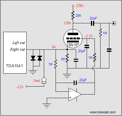
Here is the schematic and the link to the blog where he discusses this topic is here...
http://www.tubecad.com/2006/07/blog0072.htm
My naive thoughts, because I am still relatively new here, is to replace the 20K plate resistor with the top half of a mu stage. I will have to read and ponder some more about your ideas on turning it into a tube opamp.
Thanks Josh,
Well, that’s simple enough. The problem is that the input resistance (the cathode) is still pretty high because he doesn’t use feedback. The cathode gives about 770 ohms, which is in parallel with the 60 ohm resistor, for a combined resistance of 55 ohms. The PCM63, for example, has a current output port resistance of 670 ohms, lower than you’d think. It expects to drive a load much lower than that (a virtual ground) to ensure accuracy of the D-to-A conversion. 55 ohms is still a large portion of 670 ohms, better than 100 ohms, but I would want lower still.
I now notice that Broskie calls out the TDA1541 for the DAC. Its output resistance is not specified in the data sheet, but the data sheet for the “A” version says this: “To ensure no performance losses, permitted output voltage compliance is ±25 mV maximum.” Since it puts out 4mA at peak, this means that the load resistance must be lower than 6.25 ohms for the DAC to work to spec. I expect this is typical for most current-output DACs.
- Status
- This old topic is closed. If you want to reopen this topic, contact a moderator using the "Report Post" button.
- Home
- Amplifiers
- Tubes / Valves
- 5842 grounded grid