Are you really sure that you want to use 6BM8´s here?
Right now I am thinking that seperate tubes is a better idea. I also think that I can get better performance that way. I may need a second gain stage anyway.
When I see backwards zener I think voltage regulation.  You're right, the 1st MOSFET will act as a source follower to the bias applied to it (from the divider from +V), thus the 1st stage plate voltage will be dependant on that divider. Current is set by the bottom tube's impedance (which is varied by cathode bias).
Um... but if the gate is to be negative wrt source (bah, enhancement you say? I always assume depletion mode...), the zener will again short it to +/- zener voltage and forward voltage respectively! That is to say, if the MOSFET needs -3V bias, it will be limited to -.6V by the zener in forward conduction.
If M2 is an enhancement mode FET, it will be positively biased by either the R10/R11 divider or R10 + D2 (as a zener-regulated voltage).
And yes, the pentode needs grid voltage As long as R14 = R15, you can remove C2 and direct couple it.
Tim
You're right, the 1st MOSFET will act as a source follower to the bias applied to it (from the divider from +V), thus the 1st stage plate voltage will be dependant on that divider. Current is set by the bottom tube's impedance (which is varied by cathode bias).Um... but if the gate is to be negative wrt source (bah, enhancement you say? I always assume depletion mode...), the zener will again short it to +/- zener voltage and forward voltage respectively! That is to say, if the MOSFET needs -3V bias, it will be limited to -.6V by the zener in forward conduction.
If M2 is an enhancement mode FET, it will be positively biased by either the R10/R11 divider or R10 + D2 (as a zener-regulated voltage).
And yes, the pentode needs grid voltage
As long as R14 = R15, you can remove C2 and direct couple it.Tim
Tim, let's see if I can keep the confusion going here.
The MOSFETs require a few volts + bias in order to conduct. If the gate ever fell below the source voltage (necessary condition for forward bias of the zener) the transistor would turn off and no current would flow through the tube. So lets say the G-S voltage is 4V at zero signal and zener is 12V. As long as signal isn't large enough to drive the MOSFET into cutoff the zener will do nothing. If something goes terribly wrong and the gate becomes reverse biased the zener will limit the reverse bias to about half a volt. If a transient or static charge becomes applied to the gate the zener will limit this to 12V thus protecting the MOSFET from damage. (I don't have the zener in backwards do I???)
So the trick is to set all of the circuit componant values so that when the gate of M1 is at B+/2 the source current is the desired value and the source to gate voltage is large enough to accomodate the current sense signal developed across R3 right?
Now if I remove the coupling capacitor the grid of the pentode will be at about B+/2. If I put a source resistor on M2 of an appropriate value then the current through M2 and the pentode will develop a voltage which when added to the D-S voltage of M2 will set the operating point of the pentode. So Rs and Ik would be adjusted to raise the cathode of the pentode sufficiently above the grid voltage. Also with the coupling cap removed R4 and R8 become redundantand I only need one. Have I got it right?
If they're depletion mode (off at 0Vgs) it'll work as long as the zeners are rated at a voltage greater than the necessary bias (all of what, 2V? 5V zeners ought to work fine then). But above you said:
Enhanced current flow means negative gate voltage to cut it off, just like a tube. So what the heck are these things already!!?!?!!?
Tim
Since the MOSFET is enhancement mode the source should never be more positive than the gate (unless I really goofed up somehow).
Enhanced current flow means negative gate voltage to cut it off, just like a tube. So what the heck are these things already!!?!?!!?
Tim
Communication breaking down
We will get this yet I am commited to it.
I am talking about enhancement mode (standard) N-Channel MOSFET like (just pulling one out of thin air) the data sheet attached. For E mode N channel the gate must be positive with respect to the source in order to conduct. When the gate falls below the critical voltage and/or goes negative with respect to the source the current stops flowing. This is what I am calling cut off. I apologize if that is the wrong term.
Sch3mat1c said:If they're depletion mode (off at 0Vgs) it'll work as long as the zeners are rated at a voltage greater than the necessary bias (all of what, 2V? 5V zeners ought to work fine then). But above you said:
Since the MOSFET is enhancement mode the source should never be more positive than the gate (unless I really goofed up somehow).
Enhanced current flow means negative gate voltage to cut it off, just like a tube. So what the heck are these things already!!?!?!!?
Tim
We will get this yet I am commited to it.
I am talking about enhancement mode (standard) N-Channel MOSFET like (just pulling one out of thin air) the data sheet attached. For E mode N channel the gate must be positive with respect to the source in order to conduct. When the gate falls below the critical voltage and/or goes negative with respect to the source the current stops flowing. This is what I am calling cut off. I apologize if that is the wrong term.
Attachments
 Alright so where the hell did I get this:
depletion mode (off at 0Vgs)
Enhanced current flow means negative gate voltage to cut it off,
Anyway... if you're talking the +V to turn on type stuff... the mu follower will work as advertized. The CF CCS needs a source resistor yet though (and you can remove the other voltage divider resistor, R11 was it?) so the zener D2 acts as a regulator. In this way, it gains NFB, stabilizing the drain curve (of constant current) and letting the current be set easily by the resistor value rather than gate bias, which with Gm in the mhos range (not micromhos) isn't as easy.
Tim
Designing the output stage
Primary question... How do you predict power output and distortion for CF with active load. If I had appropriate curves I could figure it out for resistive load but with CCS????
I have been looking at data sheets for possible output devices including KT88, EL509, and EL34. I noticed some interesting things.
The data sheets usually have a table listing "typical" class A design parameters followed by some characteristic curves. What is odd is that the curves almost never use the same screen voltage as the tabular design information. The strangest one is the Svetlana EL 509 which has curves for a screen voltage of 140V and a tabular design for a screen voltage of 280V. The curves go down to a grid voltage of -40V but the design uses a grid bias of -82V. So I am having a hard time getting a handle on what tubes might be appropriate and how to bias.
I was planning to use a 6N1P (Mu of 33) as the voltage amplification stage so assuming 1V p-p input a grid bias of -17V on the output stage would have adequate room for input voltage swing. Of course that input level leaves me with just 3-5W of potentail output (no gain in the output stage). If I stuck with that design I suppose any of the above tubes would work but I don't know how I would determine optimal bias given that I am using an active load.
I presume that one increases the screen voltage to allow more grid bias. That seems to be the trend that I see in devices where curves are given for different screen bias values.
I know that the 509 will allow -82V with Vscreen of 280V but I have no curves for that value. I suspect that the other tubes can be run with higher screen voltages to get similar results but I have no published information on it.
In order to get more voltage to drive the output I considered using the second triode in the 6N1P for another gain stage but I don't think it can accept a 33V p-p input signal. So how about using a low mu power triode like the SV811-3 as a driver stage in between the 6N1P and the output tube??? That would give me a voltage of about 90V p-p going into the CF output stage.
That configuration would be...
6N1P MuStage ==> SV811-3 MuStage ==> EL509 CF Active Load
I have no idea what the power output would be given the curves that I have.
Another possibility is to use an input tube with a higher Mu (triode mode only). Any suggestions?
Primary question... How do you predict power output and distortion for CF with active load. If I had appropriate curves I could figure it out for resistive load but with CCS????
I have been looking at data sheets for possible output devices including KT88, EL509, and EL34. I noticed some interesting things.
The data sheets usually have a table listing "typical" class A design parameters followed by some characteristic curves. What is odd is that the curves almost never use the same screen voltage as the tabular design information. The strangest one is the Svetlana EL 509 which has curves for a screen voltage of 140V and a tabular design for a screen voltage of 280V. The curves go down to a grid voltage of -40V but the design uses a grid bias of -82V. So I am having a hard time getting a handle on what tubes might be appropriate and how to bias.
I was planning to use a 6N1P (Mu of 33) as the voltage amplification stage so assuming 1V p-p input a grid bias of -17V on the output stage would have adequate room for input voltage swing. Of course that input level leaves me with just 3-5W of potentail output (no gain in the output stage). If I stuck with that design I suppose any of the above tubes would work but I don't know how I would determine optimal bias given that I am using an active load.
I presume that one increases the screen voltage to allow more grid bias. That seems to be the trend that I see in devices where curves are given for different screen bias values.
I know that the 509 will allow -82V with Vscreen of 280V but I have no curves for that value. I suspect that the other tubes can be run with higher screen voltages to get similar results but I have no published information on it.
In order to get more voltage to drive the output I considered using the second triode in the 6N1P for another gain stage but I don't think it can accept a 33V p-p input signal.
So how about using a low mu power triode like the SV811-3 as a driver stage in between the 6N1P and the output tube??? That would give me a voltage of about 90V p-p going into the CF output stage.That configuration would be...
6N1P MuStage ==> SV811-3 MuStage ==> EL509 CF Active Load
I have no idea what the power output would be given the curves that I have.
Another possibility is to use an input tube with a higher Mu (triode mode only). Any suggestions?
Re: Designing the output stage
First of all, when you graph the resistive load, does that mean just the resistor below the cathode, or it in parallel with the load?
Otherwise, just draw a horizontal line at the current the CCS is set to (duh, constant bias current ), find the voltage you'll bias at (probably 1/2B+) and you'll find the grid voltage (usually negligible due to the nature of a CF but for output you may be interested in the 10-20V). Now on this point, draw the loadline corresponding to your load impedance (or find what's best suited to base your OPT selection on).
Yup. It's a sweep tube, not designed for audio operation. I doubt the shown operating point is even class A anyway, though Idunno about Svet. Their sheet may be new enough to have audio ranges present. Something like a GE or Philips sheet from Frank's sheets (circa 50s-70s) would be unlikely to have any operating information besides a few common ballpark figures for sweep output.
In these situations, you have to look at the effect screen voltage has on plate current. First, as voltage rises, bias rises with it. Second, peak plate current (at 0Vg) rises. This is easily seen from the Vg=0V, Vs=100, 125, 150...V curves. It probably isn't exact but you can imagine screen voltage as scaling the current level, i.e. vertical scale of the plate curves. However, saturation voltage (where screen current drops to sane levels and plate resistance increases to CCS levels) also increases, so it really scales up both.
You get the same effect by increasing grid voltage, but your circuit expects screen current; you often have to use special techniques to account for the sudden grid current when driven positive.
The problem with a CF output, and why it's never used except extraordinary circumstances, is because it requires such dramatic drive voltage. Due to the NFB you can easily drive it with a 12AX7 (CF = high impedance input) though. I'd rather use a pentode (6AU6 or so, but I suppose a more gourmet 6267 or ... eh, what's that, 5674? no... would work fine) because they have more distinct saturation and cutoff points; distortion is higher, but drive is capable of some signal in the output stage.
To know how much power you have given an input voltage, you'll have to graph it. With a load impedance much lower than ideal (e.g., 600 ohms), you can get a dramatic amount of drive for very little voltage.
Consider a 6AS7 OTL output stage: it requires easily more than 100V, probably 200V (it's been a while since I checked out any designs) drive for all of what, 20V output?
No, screen allows lower load resistances (higher current), within ratings (Ipmax, Pdmax) of course.
To keep averages lower, grid bias can be increased, but you leave class A. For instance, you might use EL34s at 300/300V class A for oh... 20W PP? Dropping the load from say 6k to 4k (I'm guessing), increasing screen voltage to maybe 400V (and plate to 400 or 450 because it's nice to the tubes) and dropping grid bias by maybe 20V (putting them say -40V), you suddenly find yourself in class AB with 70W available. Maximum current draw has risen of course (though the tubes are still within ratings).
You can extrapolate the Vg=0V curves, mimicking the existing pattern (current rises approx 3/2 power I would presume) shown and extrapolating to 280V or whatever. A tube like that does 2 or 3A peak in such a situation I bet. Basically, find the Gm of the screen (plate current rises maybe 50mA for +25Vs; Gm = .05/25 = 2,000umhos) and extrapolate up a few volts past whatever's the top line.
Oh- I forgot, grid Gm stays kinda constant - when I'm graphing at a Vs different from that shown on the plate curves, I knock off a few curves and call the next closest one Vg=0V. For instance, if a graph says Vs=150V and I need it at 100V, I check the Vg=0V graph for what current level the 100V curve looks like, then go back and find which curve, say Vg=-5V lines up best. I then call that curve Vg=0V and in this case, each curve is 5V off; the curve shown at Vg=-15V is actually -10 in the circuit.
That's why you don't push the first triode all the way. Obviously, that doesn't work. What happens is the first tube never gets ANYWHERE AT ALL near maximum.
This actually makes things easier in some situations, for instance you can assume the plate voltage will never be out of a certain limit, else the circuit won't work (the following tube will be either cutoff or saturated; see my active preamp schematic for more on this).
I'd use a pentode, simply because you get more voltage output. You'll get massive gain and may want some local NFB, which may not be too easy so global NFB may be necessary. But then, I would never use a CF for output power anyway.
Tim
mashaffer said:Primary question... How do you predict power output and distortion for CF with active load. If I had appropriate curves I could figure it out for resistive load but with CCS????
First of all, when you graph the resistive load, does that mean just the resistor below the cathode, or it in parallel with the load?
Otherwise, just draw a horizontal line at the current the CCS is set to (duh, constant bias current
), find the voltage you'll bias at (probably 1/2B+) and you'll find the grid voltage (usually negligible due to the nature of a CF but for output you may be interested in the 10-20V). Now on this point, draw the loadline corresponding to your load impedance (or find what's best suited to base your OPT selection on).The data sheets usually have a table listing "typical" class A design parameters followed by some characteristic curves. What is odd is that the curves almost never use the same screen voltage as the tabular design information. The strangest one is the Svetlana EL 509 which has curves for a screen voltage of 140V and a tabular design for a screen voltage of 280V.
Yup. It's a sweep tube, not designed for audio operation. I doubt the shown operating point is even class A anyway, though Idunno about Svet. Their sheet may be new enough to have audio ranges present. Something like a GE or Philips sheet from Frank's sheets (circa 50s-70s) would be unlikely to have any operating information besides a few common ballpark figures for sweep output.
The curves go down to a grid voltage of -40V but the design uses a grid bias of -82V. So I am having a hard time getting a handle on what tubes might be appropriate and how to bias.
In these situations, you have to look at the effect screen voltage has on plate current. First, as voltage rises, bias rises with it. Second, peak plate current (at 0Vg) rises. This is easily seen from the Vg=0V, Vs=100, 125, 150...V curves. It probably isn't exact but you can imagine screen voltage as scaling the current level, i.e. vertical scale of the plate curves. However, saturation voltage (where screen current drops to sane levels and plate resistance increases to CCS levels) also increases, so it really scales up both.
You get the same effect by increasing grid voltage, but your circuit expects screen current; you often have to use special techniques to account for the sudden grid current when driven positive.
I was planning to use a 6N1P (Mu of 33) as the voltage amplification stage so assuming 1V p-p input a grid bias of -17V on the output stage would have adequate room for input voltage swing. Of course that input level leaves me with just 3-5W of potentail output (no gain in the output stage). If I stuck with that design I suppose any of the above tubes would work but I don't know how I would determine optimal bias given that I am using an active load.
The problem with a CF output, and why it's never used except extraordinary circumstances, is because it requires such dramatic drive voltage. Due to the NFB you can easily drive it with a 12AX7 (CF = high impedance input) though. I'd rather use a pentode (6AU6 or so, but I suppose a more gourmet 6267 or ... eh, what's that, 5674? no... would work fine) because they have more distinct saturation and cutoff points; distortion is higher, but drive is capable of some signal in the output stage.
To know how much power you have given an input voltage, you'll have to graph it. With a load impedance much lower than ideal (e.g., 600 ohms), you can get a dramatic amount of drive for very little voltage.
Consider a 6AS7 OTL output stage: it requires easily more than 100V, probably 200V (it's been a while since I checked out any designs) drive for all of what, 20V output?
I presume that one increases the screen voltage to allow more grid bias. That seems to be the trend that I see in devices where curves are given for different screen bias values.
No, screen allows lower load resistances (higher current), within ratings (Ipmax, Pdmax) of course.
To keep averages lower, grid bias can be increased, but you leave class A. For instance, you might use EL34s at 300/300V class A for oh... 20W PP? Dropping the load from say 6k to 4k (I'm guessing), increasing screen voltage to maybe 400V (and plate to 400 or 450 because it's nice to the tubes) and dropping grid bias by maybe 20V (putting them say -40V), you suddenly find yourself in class AB with 70W available. Maximum current draw has risen of course (though the tubes are still within ratings).
I know that the 509 will allow -82V with Vscreen of 280V but I have no curves for that value. I suspect that the other tubes can be run with higher screen voltages to get similar results but I have no published information on it.
You can extrapolate the Vg=0V curves, mimicking the existing pattern (current rises approx 3/2 power I would presume) shown and extrapolating to 280V or whatever. A tube like that does 2 or 3A peak in such a situation I bet. Basically, find the Gm of the screen (plate current rises maybe 50mA for +25Vs; Gm = .05/25 = 2,000umhos) and extrapolate up a few volts past whatever's the top line.
Oh- I forgot, grid Gm stays kinda constant - when I'm graphing at a Vs different from that shown on the plate curves, I knock off a few curves and call the next closest one Vg=0V. For instance, if a graph says Vs=150V and I need it at 100V, I check the Vg=0V graph for what current level the 100V curve looks like, then go back and find which curve, say Vg=-5V lines up best. I then call that curve Vg=0V and in this case, each curve is 5V off; the curve shown at Vg=-15V is actually -10 in the circuit.
In order to get more voltage to drive the output I considered using the second triode in the 6N1P for another gain stage but I don't think it can accept a 33V p-p input signal.
That's why you don't push the first triode all the way.
Obviously, that doesn't work. What happens is the first tube never gets ANYWHERE AT ALL near maximum.This actually makes things easier in some situations, for instance you can assume the plate voltage will never be out of a certain limit, else the circuit won't work (the following tube will be either cutoff or saturated; see my active preamp schematic for more on this).
Another possibility is to use an input tube with a higher Mu (triode mode only). Any suggestions? [/B]
I'd use a pentode, simply because you get more voltage output. You'll get massive gain and may want some local NFB, which may not be too easy so global NFB
may be necessary. But then, I would never use a CF for output power anyway. Tim
Thanks for all the great info
(smacks forehead) of course (feeling silly) the AC load line includes the input impedence of the output xformer in parallel with the "infinite" impedence of the CCS.
It will take a while to digest the rest. In the meantime for your reading pleasure the back page of the 509 data sheet. Hmm... enhanced triode is interesting.
First of all, when you graph the resistive load, does that mean just the resistor below the cathode, or it in parallel with the load?
(smacks forehead) of course (feeling silly) the AC load line includes the input impedence of the output xformer in parallel with the "infinite" impedence of the CCS.
It will take a while to digest the rest. In the meantime for your reading pleasure the back page of the 509 data sheet. Hmm... enhanced triode is interesting.
Attachments

mashaffer said:The EL34 is the only one that shows screen grid curves.
And even then not really, that's transfer curves.
http://www.mif.pg.gda.pl/homepages/frank/sheets/129/e/EL34.pdf
Pages 7 and 9 being the most useful. Hmm, let's try a Philips:
http://www.mif.pg.gda.pl/homepages/frank/sheets/030/e/EL34.pdf
Wtf... it's like none of them have the screen curves... and of course there's no American datasheet (6CA7).
Geez, they aren't available ANYWHERE! Global conspiracy or something... what the heck!
Anyway, how about EL509...
Plate curves for a few screen voltages but none of variable screen voltage:
http://www.mif.pg.gda.pl/homepages/frank/sheets/010/p/PL509.pdf
Nothing more on equivalents (6KG6(A), E/PL519).
KT88... FINALLY
http://www.mif.pg.gda.pl/homepages/frank/sheets/084/k/KT88.pdf
Page 6 has the curves I'm talking about.
Tim
Going back
Hey Tim;
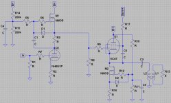
I would like to go back and revisit a couple of things. I have attached the circuit diagram with some changes.
It is still a two stage design but you will notice that I changed it to direct coupled as recommended. I want to work out the details of the output stage and then I will go back and look at the best way to drive it.
I have added the connections for the other grids on the pentode(more on that later) and a source resistor for M2.
Do R17 and C6 accomplish this? R17 is a screen stop resistor connecting the screen to an appropriate voltage to be chosen later. I suppose it would be good to make this a fairly well regulated supply. The idea behind C6 is to allow the screen to follow the AC signal at the cathode so that Vs=Vscrn+Vk.
My diagram still has R11 in it. I want to understand what you are propsing here. I have D2 as a gate protection device only at this point (I suppose it could go directly from gate to source instead of including GS resistor). Are you proposing that the tail of the D2 go to the tail of the source resistor (i.e. ground)? I see that as long as the source current is high enough that the Zener would set the current through the source resistor and thus do double duty (protection and constant current) but since the cathode voltage needs to be several tens of volts above B+/2 it would need to be a large zener string or we would need two resistors in the source circuit with the tail of D2 connected between them. Is this what you have in mind or am I missing your point?
Also I am rying to understand how to set the source resistor values to place the cathode of U1 at the desired bias point. When used as a CCS is the resistance drain to source a known constant value (on state resistance) so that the drain to source voltage would be current times drain to source resistance or would the voltage drop across M2 be determined some other way (current through tube determining grid to cathode voltage for example)? I am sorry that I am so thick at times but I really appreciate your patient tutoring.
Hey Tim;
I would like to go back and revisit a couple of things. I have attached the circuit diagram with some changes.
It is still a two stage design but you will notice that I changed it to direct coupled as recommended. I want to work out the details of the output stage and then I will go back and look at the best way to drive it.
I have added the connections for the other grids on the pentode(more on that later) and a source resistor for M2.
Pentode and tetrodes, when carelessly put in a CF circuit, are in triode mode. You need special circuitry to keep the screen at constant voltage to the cathode for it to run in true pentode mode.
Do R17 and C6 accomplish this? R17 is a screen stop resistor connecting the screen to an appropriate voltage to be chosen later. I suppose it would be good to make this a fairly well regulated supply. The idea behind C6 is to allow the screen to follow the AC signal at the cathode so that Vs=Vscrn+Vk.
The CF CCS needs a source resistor yet though (and you can remove the other voltage divider resistor, R11 was it?) so the zener D2 acts as a regulator. In this way, it gains NFB, stabilizing the drain curve (of constant current) and letting the current be set easily by the resistor value rather than gate bias, which with Gm in the mhos range (not micromhos) isn't as easy.
My diagram still has R11 in it. I want to understand what you are propsing here. I have D2 as a gate protection device only at this point (I suppose it could go directly from gate to source instead of including GS resistor). Are you proposing that the tail of the D2 go to the tail of the source resistor (i.e. ground)? I see that as long as the source current is high enough that the Zener would set the current through the source resistor and thus do double duty (protection and constant current) but since the cathode voltage needs to be several tens of volts above B+/2 it would need to be a large zener string or we would need two resistors in the source circuit with the tail of D2 connected between them. Is this what you have in mind or am I missing your point?
Also I am rying to understand how to set the source resistor values to place the cathode of U1 at the desired bias point. When used as a CCS is the resistance drain to source a known constant value (on state resistance) so that the drain to source voltage would be current times drain to source resistance or would the voltage drop across M2 be determined some other way (current through tube determining grid to cathode voltage for example)? I am sorry that I am so thick at times but I really appreciate your patient tutoring.
Attachments
Re: Going back
R8 can now be removed as the pentode's bias is set by the operating point of the first stage; it accomplishes "grid leak" automatically. Here it just loads the circuit. You can leave R9 I guess.
Oh *bites tounge*
Correct. Mind you R17 (assuming an AC-grounded supply end, which I would hope it is!) loads the output, so try to make it high. Ideally it would be a CCS, though that doesn't account for changes in screen current; a floating supply (screen to cathode) would be better, but whaddya gonna do.
Doubt you're going to go much past class A in this thing anyway.
I suggest a constant voltage supply, i.e. regulated by the diode, which feeds the gate. This biases it on, causing voltage on R16 to rise; the MOSFET wells up and starts turning off. Ultimately it sets a constant current point once the voltage settles (within microseconds I'm sure). The resistor also causes NFB, making it more constant. Should be up in the 10s of megohms.
Yep!
As a result, R11 is just stealing current from the reg so you can omit it.
Eh? The source/gate end is isolated from the drain/cathode end.
You can do it the reciprocal method of the driver stage using P-channel MOSFETs, but upside-down P channel/PNP stuff is even more confusing until you get used to it.
As the tube is a follower, its cathode will be [bias] number of volts above its grid; nothing can change this. MOSFET is only there to set current.
Rds(on) is a figure that only tells you how much current you can sink at an approx. Vds or vice versa. When used as a switch. For instance, if you're sinking 50A, you want something in the miliohm range. Meaningless for any analog circuit like this.
The voltage drop across M2 (really should be Q2, but whatever) is (driver plate) - (output bias) - (source resistor), where (output bias) is Vgk and a negative number. Say driver is biased to 150V and the MOSFET is set to say, 40mA. Given +300V screen, the EL34 might bias -10V and MOSFET at maybe 2 or 3V. Hence it'll have 150 - (-10) - 3 = 137V across it. It will dissipate 5.5W. Just a SWAG, though I'd like to know how close it is.
Tim
mashaffer said:It is still a two stage design but you will notice that I changed it to direct coupled as recommended.
R8 can now be removed as the pentode's bias is set by the operating point of the first stage; it accomplishes "grid leak" automatically. Here it just loads the circuit.
You can leave R9 I guess.I want to work out the details of the output stage and then I will go back and look at the best way to drive it.
Oh *bites tounge*
Do R17 and C6 accomplish this? R17 is a screen stop resistor connecting the screen to an appropriate voltage to be chosen later. I suppose it would be good to make this a fairly well regulated supply. The idea behind C6 is to allow the screen to follow the AC signal at the cathode so that Vs=Vscrn+Vk.
Correct. Mind you R17 (assuming an AC-grounded supply end, which I would hope it is!) loads the output, so try to make it high. Ideally it would be a CCS, though that doesn't account for changes in screen current; a floating supply (screen to cathode) would be better, but whaddya gonna do.
Doubt you're going to go much past class A in this thing anyway.
My diagram still has R11 in it. I want to understand what you are propsing here.
I suggest a constant voltage supply, i.e. regulated by the diode, which feeds the gate. This biases it on, causing voltage on R16 to rise; the MOSFET wells up and starts turning off. Ultimately it sets a constant current point once the voltage settles (within microseconds I'm sure). The resistor also causes NFB, making it more constant. Should be up in the 10s of megohms.
Are you proposing that the tail of the D2 go to the tail of the source resistor (i.e. ground)?
Yep!
As a result, R11 is just stealing current from the reg so you can omit it.
I see that as long as the source current is high enough that the Zener would set the current through the source resistor and thus do double duty (protection and constant current) but since the cathode voltage needs to be several tens of volts above B+/2 it would need to be a large zener string or we would need two resistors in the source circuit with the tail of D2 connected between them. Is this what you have in mind or am I missing your point?
Eh? The source/gate end is isolated from the drain/cathode end.
You can do it the reciprocal method of the driver stage using P-channel MOSFETs, but upside-down P channel/PNP stuff is even more confusing until you get used to it.
Also I am rying to understand how to set the source resistor values to place the cathode of U1 at the desired bias point.
As the tube is a follower, its cathode will be [bias] number of volts above its grid; nothing can change this. MOSFET is only there to set current.
When used as a CCS is the resistance drain to source a known constant value (on state resistance) so that the drain to source voltage would be current times drain to source resistance or would the voltage drop across M2 be determined some other way (current through tube determining grid to cathode voltage for example)?
Rds(on) is a figure that only tells you how much current you can sink at an approx. Vds or vice versa. When used as a switch. For instance, if you're sinking 50A, you want something in the miliohm range. Meaningless for any analog circuit like this.
The voltage drop across M2 (really should be Q2, but whatever) is (driver plate) - (output bias) - (source resistor), where (output bias) is Vgk and a negative number. Say driver is biased to 150V and the MOSFET is set to say, 40mA. Given +300V screen, the EL34 might bias -10V and MOSFET at maybe 2 or 3V. Hence it'll have 150 - (-10) - 3 = 137V across it. It will dissipate 5.5W. Just a SWAG, though I'd like to know how close it is.
Tim
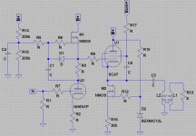
Like this?
So we want a setup like this right? Thats a 12V zener and 300 ohm source resistor ==> 40mA right? The 40mA through the tube sets the voltage between grid and cathode by the tube characteristics. Voltage across MOSFET is what ever is left. Have I got it now?
For the input stages as I see it at the moment we have three choices of choices.
- Single high Mu CC voltage amplifier to get gain close to 100.
- Two CC stages with a low gain first stage and Mu-Stage for the second stage. I might be able to find a low Mu preamp triode for the first stage that would allow using Mu-Stage there too but I haven't looked yet.
- Use preamp tube for the first tube and low Mu power tube as second tube both run as Mu-Stage. The power tube would not be working very hard at all of course and I don't know how this would affect distortion. It seems like it should do OK as long as I bias it with enough DC current to keep it happy.
[/list=1]
In solution 1 I would be concerned about distortion if I had to use a pentode to get the needed gain. In solution 2 I think that the best distortion would be acheived with Mu-Stage on both but this would require just the right cmbination of Mu's for the two tubes making the choice of tubes possibly a bit tricky. For solution 3 I know of two tubes that will give the right gain figures (Mu of 33 and Mu of 3.5) but what I don't know is whether the use of a power triode as the driver is a problem and whether there are any disadvantages to having the high gain tube first (as long as the power triode can handle the 35V p-p input).
And then there's DHT Class A2 Cathode drive
This CF Pentode archetecture that we have been discussing was chosen because of the potentially higher damping and the pentode's tendancey to be more linear in CF mode. On the other hand I am becoming rather intrigued by what I have been reading about using direct heated triodes in class A2 operation with 0V grid bias and cathode drive. In applications where high damping factor is not critical this arrangement might have some advantages. What do you all think? The CCS loaded CF circuit we have been looking at could even be used as a driver for a class A2 output stage couldn't it?
This CF Pentode archetecture that we have been discussing was chosen because of the potentially higher damping and the pentode's tendancey to be more linear in CF mode. On the other hand I am becoming rather intrigued by what I have been reading about using direct heated triodes in class A2 operation with 0V grid bias and cathode drive. In applications where high damping factor is not critical this arrangement might have some advantages. What do you all think? The CCS loaded CF circuit we have been looking at could even be used as a driver for a class A2 output stage couldn't it?
A while ago I came up with this circuit consisting of one 6DJ8, one plate choke for the above, one P channel power mosfet and one 811A positive bias DHT.
The 6DJ8 was driving the mosfet which was connected as a follower between the 811´s cathode and ground = cathode drive.
A quite clever topology if I may say it myself, everything was direct coupled and the bias for the output tube would be set by the DC drop across the 6DJ8´s plate choke + the Vgs of the mosfet. Since the 811 requires positive bias (and thus draws grid current all the time) a lost bias voltage would result in cutoff rather than runaway.
Maybe I should mention that I never tried the circuit practically, but maybe I will some day.
- Status
- This old topic is closed. If you want to reopen this topic, contact a moderator using the "Report Post" button.
- Home
- Amplifiers
- Tubes / Valves
- Experiences with White CF/CCS CF output stage