Hi
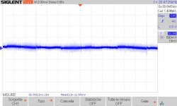
in attach the test on FFT by AP about the HT voltage just after the bridge, around 350 vdc with 330 uF as filter cap and bridge of 25A.
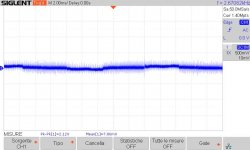
Then at the output of HT stabilized circuit I normally use.
The current is 20 mA ( is a line tube stage).
The results is interesting.
The attenuation on region from 30 to 2kHz is very fine.
At 100 hz the difference of the two peaks is 100 dB; same for the other multiplies (less or more)
Personally in each stage, line or phono, I use this one because it helps a lot also for s7n.
In additon the screenshot from scope on wave at input of board, in out and the residual
Walter
in attach the test on FFT by AP about the HT voltage just after the bridge, around 350 vdc with 330 uF as filter cap and bridge of 25A.
Then at the output of HT stabilized circuit I normally use.
The current is 20 mA ( is a line tube stage).
The results is interesting.
The attenuation on region from 30 to 2kHz is very fine.
At 100 hz the difference of the two peaks is 100 dB; same for the other multiplies (less or more)
Personally in each stage, line or phono, I use this one because it helps a lot also for s7n.
In additon the screenshot from scope on wave at input of board, in out and the residual
Walter
Attachments

Walter,
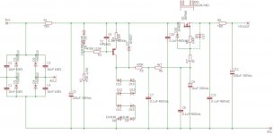
I really appreciate that you are writing this up with “English as a 2nd language”. However, I also feel that you posting a circuit diagram would more helpful than the words you wrote. Especially if you label the circuit diagram with the “test points” you show the oscillograms and FFTs for.
Thanks in advance,
⋅-=≡ GoatGuy ✓ ≡=-⋅
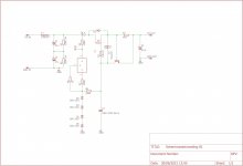
Ops!
The input is on B+L and out is HTLout
The diagram is one channel. The board is dual.
There is the possibility to mount on board the bridge or directly a rectified voltage; in this case I get the voltage from an externl source + bridge + 330uF +220 uF on board.
Walter
The input is on B+L and out is HTLout
The diagram is one channel. The board is dual.
There is the possibility to mount on board the bridge or directly a rectified voltage; in this case I get the voltage from an externl source + bridge + 330uF +220 uF on board.
Walter
Attachments
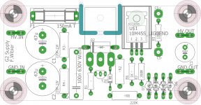
Im curious as to why you included four 1n4148 in series with the zener stack, is this some sort of temperature stabilisation?
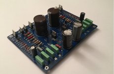
Very nice project, and well thought out schematic. I like how you placed reverse polarity diodes nearly everywhere.
Just a little tip i got from someone, if you make the drill size of your solder pad 1.9mm, you can fit a 2mm banana connector. so you can test without soldering. Personally i prefer fastons.
Below is my version if you need more ideas.
Attachments

Hi
the 4148 are for temperature.
Regarding the drill size, normally I use a terminal with screw for semplicity and have the possibility to use different cables diameters.
I tested this circuit with around 250-300 Volts out and 300 mA rms max and I lost around 1 volt
The IRF840 works fine but the STP10NK80Z are also fine with internal protection
Walter