I am attempting to restore a vintage amplifier. The original PCBs were destroyed. I thought this would be a good opportunity to learn, so I attempted to improve the layout, in particular the grounding scheme.
Please let me know what you think! About any of it, but in particular the grounding.
I did a lot of reading, but I'm not at the point where I have integrated everything I learned. So I'm not terribly confident in my understanding of how everything interacts as a system.
I attached:
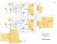
1.) The Schematic: Everything in yellow is off-board. Each channel has its own identical board, so for simplicity, let's use Channel A as the reference.
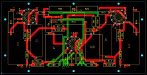
2.) My Layout: Green is ground, it is on the top layer. Red is everything else, it is on the bottom of the board. I tried to keep all the traces as short as possible and to keep the loop between signal and return as tiny as possible. Some traces are top each other (signified by the dashed red lines).
3.) A Drawing of the Board Hooked Up I thought it would be helpful to see how the board will be wired into the amp.
Please let me know what you think! About any of it, but in particular the grounding.
I did a lot of reading, but I'm not at the point where I have integrated everything I learned. So I'm not terribly confident in my understanding of how everything interacts as a system.
I attached:
1.) The Schematic: Everything in yellow is off-board. Each channel has its own identical board, so for simplicity, let's use Channel A as the reference.
2.) My Layout: Green is ground, it is on the top layer. Red is everything else, it is on the bottom of the board. I tried to keep all the traces as short as possible and to keep the loop between signal and return as tiny as possible. Some traces are top each other (signified by the dashed red lines).
3.) A Drawing of the Board Hooked Up I thought it would be helpful to see how the board will be wired into the amp.
Attachments
Last edited:
Looks like more clearance would be good at a number of places, like near SX4.
You need at least 1mm clearance for most tube circuit voltages. It may be necessary
in some places to narrow the trace width to get enough clearance.
Thanks! Good point.
The drivers (the tubes on the left and right) operate at 350V. So those traces are definitely spaced well enough.
The pre/inverter's highest voltage is 120V. So yes, some of them need more room. I'll fix that. Thank you!
If you google "PCB voltage clearance" you'll find a bunch of results, including some standards, for the minimum clearance between traces for various PCB types.
I suggest using connectors rather than just adding a pad for a wire connection.
Your traces appear enormously wide. Are you planning to fabricate this board yourself using toner transfer or similar? An outfit like OSH Park (not to mention the various Chinese outfits) will make boards for you for next to nothing. If you go with a professionally fabricated board, you can use more reasonable design rules. I generally use trace widths in the range of 8-15 mil for low-current signals.
Try to minimize the number of drills used. I generally use 32, 40, 51, and 130 mil as standard drills. I'll usually have some holes with diameters between 51 and 130 mil depending on which connectors and such that I'm using. See the manufacturer's data sheet for the recommended footprint and hole diameters.
For rectangular pins, you can calculate the needed hole diameter as diameter = sqrt(x^2+y^2)+6mil.
1 mil = 0.001" = 25.4 um.
A common route strategy is to route north/south in one layer and east/west in the other layer. I route critical signals first. Then power. Then everything else.
It looks like you have components on both sides of the board. I'd avoid that if at all possible. It'll make assembly a nightmare. In your case, there's no need for it. You could easily fit everything on one layer. The tube sockets will have to go on the opposite side if you want the tubes to poke through the top panel of the chassis. They'd be the only exception to the "single-sided assembly" rule.
Tom
Last edited:
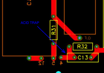
Also: You have an acid trap in your layout. Try to avoid acute angles like this one.
You want to go straight into pads if at all possible. I also tend to avoid 90º angles in traces. I don't see a point of rounded corners, unless you're dealing with RF. I use 135º corners all the time, though.
Tom
You want to go straight into pads if at all possible. I also tend to avoid 90º angles in traces. I don't see a point of rounded corners, unless you're dealing with RF. I use 135º corners all the time, though.
Tom
Attachments
Thanks for your suggestions Rayma and Tomchr. I have updated the board.
My main concern is that I've done something bone-headed that will create noise/hum, or that I missed something that can help minimize the possibility. See anything of that sort?

Changes:
1.) There is now (unless I missed anything) more than enough space between all traces and pads -- accomplished by shrinking some of the traces and tweaking the spacing here and there.
2.) I have also standardized hole/pad sizes. I have one size pad/hole for all the 1/2 watt resistors, one size and for all the large wire wound resistors, and one size for all the capacitors.
3.) I adjusted the angles of the questionable trace intersections.
A few notes on some of the other suggestions:
My main concern is that I've done something bone-headed that will create noise/hum, or that I missed something that can help minimize the possibility. See anything of that sort?
Changes:
1.) There is now (unless I missed anything) more than enough space between all traces and pads -- accomplished by shrinking some of the traces and tweaking the spacing here and there.
2.) I have also standardized hole/pad sizes. I have one size pad/hole for all the 1/2 watt resistors, one size and for all the large wire wound resistors, and one size for all the capacitors.
3.) I adjusted the angles of the questionable trace intersections.
A few notes on some of the other suggestions:
- I am not making the boards myself. I will be having them manufactured for me.
- I made the traces as thick as possible because I figured it can't hurt.
- I'm trying to to keep the same "look" as the original boards. So while I've moved a lot of pieces to optimize things, I've kept the same "massing" and "shape" of the parts, so to speak. That's why I put the big caps on the bottom of the board. Realizing this might make assembly a paint, I made sure to arrange everything so I can assemble everything, then install the caps at the very end. So assembly should not be an issue.
- Adding connectors sounds like a good idea. I'm going to add them next revision.
Last edited:
R19 overlaps C12. Even if they are mounted on opposite sides, the pad of R19 cannot be within the courtyard of C12.
In general, you have a bunch of meandering traces - straight traces between pads are preferable. The current trace widths are nice - I'm not a fan of thin traces and see no benefit to them, except when you need to reduce capacitance, but you have no copper planes so the point is moot.
There's a DECOUP GROUND trace that winds under SX5, through the pins when it could clear that socket completely by routing it to the right. Or, since it's a ground, you could convert that into a copper pour and it will act like a ground a lot better than a thin, windy trace. You may want a star ground but I find that more copper is better than slicing it into tiny ribbons that end up not acting like ground at all. If you do a pour, set the software to give you a wide clearance, maybe 20 mil. Do not go right up to the design limits of space/trace. Designing to 7 mil space/trace is fine for low voltage stuff, and 20 mil is safer for tube voltages.
When someone substitutes a box capacitor for that axial cylindrical cap, they will not have a good time. Don't let the pad enter the cap's courtyard.
In general, you have a bunch of meandering traces - straight traces between pads are preferable. The current trace widths are nice - I'm not a fan of thin traces and see no benefit to them, except when you need to reduce capacitance, but you have no copper planes so the point is moot.
There's a DECOUP GROUND trace that winds under SX5, through the pins when it could clear that socket completely by routing it to the right. Or, since it's a ground, you could convert that into a copper pour and it will act like a ground a lot better than a thin, windy trace. You may want a star ground but I find that more copper is better than slicing it into tiny ribbons that end up not acting like ground at all. If you do a pour, set the software to give you a wide clearance, maybe 20 mil. Do not go right up to the design limits of space/trace. Designing to 7 mil space/trace is fine for low voltage stuff, and 20 mil is safer for tube voltages.
I took advantage of the caps' geometry (cylinders) to avoid this issue. There's more than 1/8" clearance between the leads/joints from the top-side parts and the bottom-side capacitors.
When someone substitutes a box capacitor for that axial cylindrical cap, they will not have a good time. Don't let the pad enter the cap's courtyard.
R19 overlaps C12. Even if they are mounted on opposite sides, the pad of R19 cannot be within the courtyard of C12.
In general, you have a bunch of meandering traces - straight traces between pads are preferable. The current trace widths are nice - I'm not a fan of thin traces and see no benefit to them, except when you need to reduce capacitance, but you have no copper planes so the point is moot.
There's a DECOUP GROUND trace that winds under SX5, through the pins when it could clear that socket completely by routing it to the right. Or, since it's a ground, you could convert that into a copper pour and it will act like a ground a lot better than a thin, windy trace. You may want a star ground but I find that more copper is better than slicing it into tiny ribbons that end up not acting like ground at all. If you do a pour, set the software to give you a wide clearance, maybe 20 mil. Do not go right up to the design limits of space/trace. Designing to 7 mil space/trace is fine for low voltage stuff, and 20 mil is safer for tube voltages.
Is it desirable to clear the socket?
My rational for routing the returns (the grounds) was to keep each circuit's loop area as small as possible. So the return traces (grounds) track their circuits' respective supply traces.
Is my logic faulty?
If not, is making a plan a better way to implement it?
knarfor,
You need a circuit revision. Simple, but important. Connect each output tube's individual cathode current sense resistor directly to ground. Do not connect those through the switch. Then use a 5 position switch to connect the meter and its dropping resistor to the switch rotor, and the 4 stators to their respective cathode current sense resistors. The 5th position is Meter off, so it is not subjected to the time varying DC when audio test tones, and music is applied to the amp (current changes with signal in Class A, and even more if it goes into class AB).
If you do use your current switch scheme, be sure it is a make-before-break switch. The last thing you want is the quiescent current of one tube going to zero as the switch contact opens before the other switch contact closes. That will sound bad, and may damage a tube, OPT, tweeter, or your ear.
knarfor,
You need a circuit revision. Simple, but important. Connect each output tube's individual cathode current sense resistor directly to ground. Do not connect those through the switch. Then use a 5 position switch to connect the meter and its dropping resistor to the switch rotor, and the 4 stators to their respective cathode current sense resistors. The 5th position is Meter off, so it is not subjected to the time varying DC when audio test tones, and music is applied to the amp (current changes with signal in Class A, and even more if it goes into class AB).
If you do use your current switch scheme, be sure it is a make-before-break switch. The last thing you want is the quiescent current of one tube going to zero as the switch contact opens before the other switch contact closes. That will sound bad, and may damage a tube, OPT, tweeter, or your ear.
Thanks for this! Yes, I thought that was a particularly weak/bad part of the design. Good to get confirmation and a road map on fixing it.
For my valve amp designs I use star grounding. Don't mix output grounds with input grounds. I also keep input signal short as possible and surrounded by ground plane. On input valves keep tracks and components as near to valve as possible, especially grid stoppers.
So would Version 2 be preferable to the scheme I posted previously?
Version 1:
"Source" traces in red, "return" traces in green"

Version 2:
"Source traces are the same as in previous versions, but the "returns" are in the form of planes for each section.
The large outer plane is for the drivers. The inner left plane is for the input section. The inner right plan is for the inverter section.
Everything still connects to the rest of the circuit as indicated in the first post.

Last edited:
Any advice on the above before I randomly pick one version and have it made? Haha!
I would go with the copper pour pcb.
- Status
- This old topic is closed. If you want to reopen this topic, contact a moderator using the "Report Post" button.
- Home
- Amplifiers
- Tubes / Valves
- Please Critique my first PCB : )