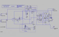
uses a jfet op amp in front end, mosfet output.
the "zener" shown is a bias circuit "shortcut".... use a bias transistor network instead. this circuit also has a DC servo and a clipping detector.
pay no attention to source V6. it's two purposes were IMD testing, and tricking the FFT in the sim into a higher resolution analysis of the output spectrum.
there's also a few "dead end" wires shown in the schematic..... i'll have a "cleaned up" copy of this available in a few days.
i think this is about ready for the prototype stage. it's a fairly simple amp, 6 transistors and an op amp.
i'm building the first prototype with +/- 15v rails for proof of concept, then i will start working up in voltage after working the bugs out of it...... looking for a gutted amp chassis (well not completely gutted.... it would be nice to find one with a working power supply and adequate heat sinks).....
don't bother looking up the p channel output device, i had to "borrow" the model of an n channel fet to get a p channel fet that was close to being a complement. i don't have the specs for the new toshiba 250 volt complementary pair transistors yet, so i had to model a complementary pair from within the mosfet library i already have.....