Hi.
I know some theory and maths about diff pairs, common emitters, common collectors, miller... But nearly nothing to connect those stage together to make an amplifier.
Should we design all stages independently, but that stage N's output has a bias voltage of x volts, that matches the N+1's input bias point? Or can the stages have different bias voltages, and current will flow between them even without signal?
One stage can output DC and, or AC into the next stage. The output impedance must match the input impedance of the next stage though. The voltage/current ratio must be the same in order for one stage to drive the next so the next stage will operate within it's specified range and so on. As for that specified range, it is determained in the design of the stage.
Say you have a VAS. This might be used to drive an emitter follower stage, with a current source bias. A 4Ohm EF stage has a beta of 250. If then the input Z of the EF stage is 1KOhms, and the peak voltage is 10V, then the VAS must be able to drive 10V at 10mA. Iq of the VAS must be greater than 10mA.
Usually you don't have to be exactly perfect in analog, altough there are perfectionists out there.
usually output stage is in class AB and previous in A (SE or p-p)
it is nice when next stage has low influance on the previous (read:high input Z, low output). sorry if you find it cliche
it is nice when next stage has low influance on the previous (read:high input Z, low output). sorry if you find it cliche
Regarding impedance matching: For optimum current transfer you want a high output impedance feeding a low input impedance. For optimum voltage transfer you want a low output impedance feeding a high input impedance.
The output impedance of a stage also affects what sort of voltage you can connect the output to. For instance a common-base stage has a very high output impedance, so you can connect it to any voltage and it won't mind (although you have to make sure to leave enough Vcb to avoid saturation). This also means you can't rely on the output voltage of such a stage to bias the next stage (which is why complementary differential amps can't have current mirror loading). On the other hand, a common-collector stage has a low output impedance, so if the bias voltage of the next stage is different from the output voltage, a large current will flow, which is not good.
The output impedance of a stage also affects what sort of voltage you can connect the output to. For instance a common-base stage has a very high output impedance, so you can connect it to any voltage and it won't mind (although you have to make sure to leave enough Vcb to avoid saturation). This also means you can't rely on the output voltage of such a stage to bias the next stage (which is why complementary differential amps can't have current mirror loading). On the other hand, a common-collector stage has a low output impedance, so if the bias voltage of the next stage is different from the output voltage, a large current will flow, which is not good.
Ok here's the problem.
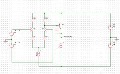
I'm trying to design an amp, a brief schematic is showed.
To have a proper bias on the VAS, R4 has to be 0.7V DC across it, right?
So I have the choice of
-very low bias for the diff pair, and a high value load resistor->high gain in the diff pair
-a few mA bias in the diff pair, but in order to have 0.7V DC on R4, R4 must be small -> low gain in the diff pair
Right? Or have I forgotten something?
Attachments

Your thinking is along the right lines and essential for open loop operation, but when overall feedback is applied by closing the loop from output to input, the LTP will do whatever it needs to maintain whatever is fed to its input, thus the VAS will be biased accordingly. This is especially true if you run a CCS on the VAS.
So I have the choice of
-very low bias for the diff pair, and a high value load resistor->high gain in the diff pair
-a few mA bias in the diff pair, but in order to have 0.7V DC on R4, R4 must be small -> low gain in the diff pair
Not necessarily so. The Diff Gain can be the same as it is a function of I and R.
Much of it depends on your VAS. If I2 is large and I1 is small, Q3 will "load" Q2 collector. With I1 small, you will also have more difficulty with C1.
Regards
Right.To have a proper bias on the VAS, R4 has to be 0.7V DC across it, right?
Start by choosing I1 and I2. The current that must flow through R4 is the collector current of Q2 minus the base current of Q3. The voltage across R4 will be about 0.6V. Divide this by the current through R4 to give the optimum value of R4. Choose the nearest convenient value.
There are two fundamental issues with the circuit as drawn.
1. The differential pair Q1 and Q2 have different polarity voltages at their bases. So Q2 is biased hard off. When biased correctly, emitter resistors allow the currents in the collectors to balance because each transistor tries to establish 0.65V across the base and emitter (Vbe). 0.65V bias is not exact and varies with each transistor, but is close with similar power devices.
2. From the above, the current through Q3 is indeterminate because the exact base voltage is not known. The current gain (the emitter current/base current) varies wildy. So even though the Vbe is around 0.65V, the current in the collector will also vary wildly. Place a resistor in the emitter and you can now calculate the current. Base voltage to rail voltage minus 0.65V gives the voltage across the emitter resistor for Q3 and hence the current. This is a determinant system with the current gain of the transistor always trying to have 0.65V (approx) from base to emitter.
Essentially this is how you link stages. You must create determinant sections where currents are known. If you know the currents, you will then know voltages at the nodes of interest. You can join stages either via voltage or current. In your case you are using voltage. Therefore earlier stages need to have enough current to supply the base current of following stages. Eg. 10 times the base current of the following stage which is determined by the current gain of the transistor. The following stage, then does not load the preceding stage and your current voltage calculations stay intact.
1. The differential pair Q1 and Q2 have different polarity voltages at their bases.
2. ...the current through Q3 is indeterminate because the exact base voltage is not known. ....
0) You are responding to a 13 year old post. Bricolo may have worked it out, or moved on.
1) Both Q1 and Q2 bases are at *zero* DC, but opposite polarity AC signals. This is appropriate for a differential input.
2) Q3 current is always exactly I2 current. As drawn, Q3 collector voltage is indeterminate, yes. However the amplifier gain is near infinite, so it can NOT be used in this form, and would surely have Negative Feedback. An appropriate connection will set Q3 collector voltage.
- Status
- Not open for further replies.
- Home
- Amplifiers
- Solid State
- Amplifier design: how to connect a stage with the next one?