While working in another project, I came across the need to build a MOS output stage based on a previous idea I later found to be already in use, more precisely in the Tiger line. Sziklai pairs as known were pointed to me by Tube Dude while AKSA provided valuable insight in his own experience with the configuration.
The first thing that struck me with the Tiger topology was the low gate source resistor values used, implying high dissipation in the driver devices. The low frequency pole caused by the high MOS input capacitance (typically 500p to 1nF depending on device size) can be pushed as in the Tiger case with a low resistor value, but this problem can be circumvented in my experience with higher overall loop gain and negative feedback, as well as mitigated by lead compensation at the driver input.
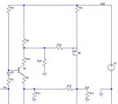
The other problem and much more serious as I was to learn in practice, is the effect of the high gate capacitance when the driver transistor goes from the off condition to on, forcing the feedback to push hard during crossover. The crossover glitch is almost impossible to overcome unless some form of standby biasing independent of driver transistor condition is applied, and this I did in the circuit shown (only upper half, the other is complementary symmetric) with resistor R20 from gate to ground for the time being, though this actual implementation cannot be considered adequate from the stability and repeatability standpoint. The lower MOS gm make this kind of source resistance stabilization (by R4) not nearly as good as the equivalent configuration with bipolar transistors (in my humble oppinion).
With this in mind, and pondering about output device protection desirably including some simple approach to SOA, I devised the circuit shown in the next posts. I do not know whether this topology has been proposed before, simulations look promising and I am planning to actually test it in the future once I have time for it.
The first thing that struck me with the Tiger topology was the low gate source resistor values used, implying high dissipation in the driver devices. The low frequency pole caused by the high MOS input capacitance (typically 500p to 1nF depending on device size) can be pushed as in the Tiger case with a low resistor value, but this problem can be circumvented in my experience with higher overall loop gain and negative feedback, as well as mitigated by lead compensation at the driver input.
The other problem and much more serious as I was to learn in practice, is the effect of the high gate capacitance when the driver transistor goes from the off condition to on, forcing the feedback to push hard during crossover. The crossover glitch is almost impossible to overcome unless some form of standby biasing independent of driver transistor condition is applied, and this I did in the circuit shown (only upper half, the other is complementary symmetric) with resistor R20 from gate to ground for the time being, though this actual implementation cannot be considered adequate from the stability and repeatability standpoint. The lower MOS gm make this kind of source resistance stabilization (by R4) not nearly as good as the equivalent configuration with bipolar transistors (in my humble oppinion).
With this in mind, and pondering about output device protection desirably including some simple approach to SOA, I devised the circuit shown in the next posts. I do not know whether this topology has been proposed before, simulations look promising and I am planning to actually test it in the future once I have time for it.
Attachments
Biasing circuit
To achieve permanent operation in the active region, a feedback mechanism is provided through the source resistor R4, Q5 and Q3. To allow use of low source resistors, it was selected the common base differential pair configuration. It is easy to see under no M1 source current, Q5 takes most of the current from R17 leaving Q3 almost cutoff and freeing M1 gate through R3 to be pulled down by R20 thus turning it into conduction. Once a voltage drop develops in the source resistor R4, Q3 begins to conduct more rising M1 gate through R3, thus closing the negative feedback loop. D4 provides a threshold to improve gain for a given current setting.
It is easy to adjust minimum device current with standard value resistors and simulations show the added circuitry has no effect on overall amplifier performance.
In the next post, the added protection circuitry.
Attachments
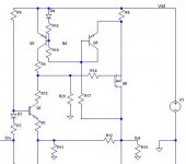
Basic protection.
With the addition of Q4 and D3, it is possible to provide current limiting and a rudimentary Safe Operating Area protection. Because of D3, Q4 starts to conduct with a voltage drop through the source resistor R4 much greater than needed by Q3 to operate the biasing loop. The basic operation is nonetheless the same, restricting source current to limit dependent on the source resistor value though finer adjustment can be achieved with added complexity.
Note R17 is not returned to a fixed voltage, but to the output itself. This way, when the output swings high when the amplifier is not loaded or loaded within nominal limits, less current is available for operating the protection, yet if the output is stuck to ground (or –V) there is much more current available, thus roughly tracking a power dissipation limit rather than strictly a current limit.
I should like to hear from members for comments about this circuit, and whether something just like this has been done before.
Rodolfo
Attachments
HI Rodolfo,
That's 1 complex circuit!!
I'm not sure that protection is altogether a good thing here....... you don't have SOAR failures with mosfets, and overcurrent is relatively easily covered with a reasonable sized fuse.
How about replacing R20 in your original diagram with a current source to the opposite rail? You could then delete R15 and R1. In fact, degeneration of the driver should not generally exceed about 22R. This will improve stability, but reduce feedback factor.
Cheers,
Hugh
The "negative drive" by R20 is a smart idea. First I read it in this Hans Hartsuiker schematic http://www.diyaudio.com/forums/attachment.php?s=&postid=560282&stamp=1106685987
Its R21-R31 there.
Cool idea, and possible of non-turnoff characteristic.
Its R21-R31 there.
Cool idea, and possible of non-turnoff characteristic.
I think that something similar to what you propose was described by Eric Margam in Wireless World sometime in the 1980s. If you're interested I can probably dig up the reference.
AKSA said:HI Rodolfo,
...you don't have SOAR failures with mosfets, and overcurrent is relatively easily covered with a reasonable sized fuse....
Yes, I expressed myself wrong, I want to address a situation where maximum current is not exceeded but because of overload, device dissipation does.
How about replacing R20 in your original diagram with a current source to the opposite rail? You could then delete R15 and R1. ..
Hugh
Replacing R20 with a current source goes a long way to make biasing independent on supply voltage. Yet I think an active biasing scheme is better suited because of the mentioned lower gm of MOSFETS. R15 is there simply for luck. (Well seriously, to divert power dissipation from Q1).
Rodolfo
lumanauw said:The "negative drive" by R20 is a smart idea. First I read it in this Hans Hartsuiker schematic http://www.diyaudio.com/forums/attachment.php?s=&postid=560282&stamp=1106685987
Its R21-R31 there.
Cool idea, and possible of non-turnoff characteristic.
Yes, I was aware of that circuit but it is for bipolars.
Also as noted, because of gate capacitante the turn on glitch is a much more serious and difficult to control issue unless a minimum operating current is always guaranteed. But the actual problem addressed with this scheme is to establish a well defined operating point.
Rodolfo
chalky said:I think that something similar to what you propose was described by Eric Margam in Wireless World sometime in the 1980s. If you're interested I can probably dig up the reference.
Yes, I should be interested to hear about it but only if it doesn't bother you too much. Thanks in advance !!
Rodolfo
Also as noted, because of gate capacitante the turn on glitch is a much more serious and difficult to control issue unless a minimum operating current is always guaranteed.
Hi, Rodolfo,
Maybe I'm thinking a little short here, but if you adjust the whole cct so it perform "not-turn-off", you won't encounter gate capacitance glitch at turn on? Because the mosfets are always on.
Hi, Rodolfo,
Maybe I'm thinking a little short here, but if you adjust the whole cct so it perform "not-turn-off", you won't encounter gate capacitance glitch at turn on? Because the mosfets are always on.
lumanauw said:....Maybe I'm thinking a little short here, but if you adjust the whole cct so it perform "not-turn-off", you won't encounter gate capacitance glitch at turn on? Because the mosfets are always on.
This is exactly the idea.
The circuit is only an attempt to provide a well controlled and stable minimum current (in the order of 50-100 mA) so the gate never sees less than the threshold voltage.
A brute force approach like the first circuit (currently in use) suffers from poor control thus forcing higher and variable quiescent currents and eventually excessive standby dissipation. For class A enthusiasts this is not an issue certainly.
Rodolfo
According to Douglas Self,
when compared to that produced from conventional class B amp toplogy, the distorsion of the output stage is not signficantly
reduced when using the so-called non-switching topologies
(such as those published by Blomley or Margam in Wireless World)
Having devices being switched to current sources
instead of being completely switched off does not cure
the distorsion problems of amplifiers with a low steady
state current
~~~~~~~~~ Forr
§§§
forr said:According to Douglas Self,
when compared to that produced from conventional class B amp toplogy, the distorsion of the output stage is not signficantly
reduced when using the so-called non-switching topologies
(such as those published by Blomley or Margam in Wireless World)
Having devices being switched to current sources
instead of being completely switched off does not cure
the distorsion problems of amplifiers with a low steady
state current
~~~~~~~~~ Forr
§§§
Great.
Should enjoy a substantiated argument either.
Rodolfo
Self makes many didactic, opinionated comments in his writings, not all of which are valid. For example, he gives casual attention to the Cdom issues of conventional Class AB PP amplifiers, yet these issues are pivotal to good sonics. This is but one area he never fully addresses (along with the mandatory use of current mirrors and sources), preferring instead to lambast the unscientific poppycock of the subjectivists and pore over his simulations.
I believe there are very good sonic benefits to keeping all outputs on at all times; if low bias instabilities, especially of the CFP topology, can be removed, I see no reason why the absence of switching artefacts would not reward with better sound. Apparently both Blomley and JLH thought the same.
Further, I have never, not even once, found that an improvement in linearity in an audio amplifier design did not result in better sound.
Thus, Rodolfo, I applaud your efforts and would encourage you to continue. A bit more simplification and you might have it.
I'm doodling as fast as I can........
Cheers,
Hugh
AKSA said:....Thus, Rodolfo, I applaud your efforts and would encourage you to continue. A bit more simplification and you might have it.
.....Hugh
Many thanks for your comments Hugh.
I'm afraid this circuit cannot be simplified too much while keeping an active control of minimum device current for reasons I will try to put as clearly as I am able to do.
To have active control, it is necessary to measure device current, and probably the easiest way is by the customary voltage drop on a series low value resistor.
We also want to control a low current (50 -200 mA or thereabouts), and at the same time do not want to have an excessive voltage drop at peak working current (5 - 10 - 20 A, whatever the design power output) depriving of maximum PSU capability and forcing excessive heat dissipation on the sensing resistor.
The combination of both requisites implies the voltage drop under quiescent condition (or during the reverse cycle when the other device is conducting) must be in the order of tens of milivolts.
To measure reliably this voltage drop, one must resort to some form of differential comparator, and for this you need at least 2 transistors.
Now you see the proposed circuit, just for quiescent current control uses exactly 2 transistors, doing for convenience the voltage comparation at the emitter side instead of at the more frequent base side.
I wish it could be made simpler, at least I have not figured out how but may be someone comes with a cool idea in this respect.
Rodolfo
Hugh (AKSA) said :
"Further, I have never, not even once, found that an improvement in linearity in an audio amplifier design did not result in better sound."
Douglas Self based his work on the simple idea that there is no instrument more sensitive than an harmonic distorsion analyser to detect the origins of non-linearities in an amplifier. He tackled a lot of them, some which were almost unknown to many designers, even of great reputation. This seems to have not pleased everybody.
Am I wrong ? I understand that Hugh's ears like high linearity, but not the one achieved by Douglas's amp which is one of the highest all over the world...
Of course, my post was not to discourage Rodolfo's project, but may just be considered as an implicit warming that he may disappointed with the results.
Among some others, I have built the Blomley, Margan and Self amplifiers. This last one (with emitter followers) is the only of the three which has not been dismantled.
~~~ Forr
§§§
forr said:...Of course, my post was not to discourage Rodolfo's project, but may just be considered as an implicit warming that he may disappointed with the results.
...
~~~ Forr
§§§
No problem and I appreciate your concern.
What Hugh wanted to emphasize is Self has proven to be controversial on some issues and this may be one. Note that what is in discussion is not a possitive affirmation by Self in the sense that some feature is better, but rather a negative affirmation in the sense that some feature does not contribute positively to the result.
Hugh makes clear linearity is the (hardly controversial) goal as much as Self does, striving for the lowest possible THD.
No cutoff operation (by brute force passive bias) solved the issue of gate capacitance induced glitch in my case, and the amplifier I was testing for a novel feedback arrangement that is my focus measures excellent.
Simulation of the active bias proposed on the other hand, makes absolutely no negative effect in linearity but it has to be tested for confirmation.
Rodolfo
Doug Self's book is a "must" read for ones who want to study audio amps. Very much technical tutorial there. But must be reminded, that this book is made by distortion meter as guidance, not with actual amplifier connected to speakers. These 2 things are usually not going in the same way.
About non-turnoff issue, I read something intersting from Kranis here http://www.diyaudio.com/forums/showthread.php?postid=561666#post561666
He wrote, that having output devices not turning off is different than having continuous forward path. This makes sense, but I also think that having output devices not turning off will also have benefit.
But, which is giving more unpleasant sound, transistor turnoff-turn-on or discontinues in forward gain?
I think it is difficult to have continuous forward gain with class AB or B.
Self belongs to a caste of audio "people" that aggravate some of their peers because they try to measure things and will not accept subjective evaluation. On the other hand the strong subjectivist faction aggravates Self and others with a like outlook.
One caution with reading Self and using his conclusions is to accept them uncriticly and over-generalize. One example: he publishes a table for EF topology output stages that associates the voltage read across a Vbe-multiplier with the voltage across the RE-resistors. The book suggests this is universal and it may well be within the limited universe of his non-symetrical blameless topology. I am personally certain that the relationship doesn't hold in the case of at least one similar but symetrical IS and VAS topology. Trying to apply his Vbe voltage setting to thisparticular case results in drastic over-biasing.
The second caution is that some of his preferences such as for CFB output topology may be valid if like Self you have time money and experience to overcome the temdency to oscillate. An EF topology may have slightly higher THD but a DIYer is more likely to produce a stable (non-oscillating result).
One thing I especially like about his approach is that he makes few claims that he has not personally investigated. Too many other audio writers just repeat received "knowledge". In this regard, he encourafes me to test out some of the common assertions as well as his own. I don't have the equipment or experience to do this to a great degree, but when I can I try to confirm things for myself.
There is conflicting information on his website regarding this issue. On the one hand, where he compares topologies he seems to favour the Sziklai (or CFP, whichever you prefer to call it). On the other hand, sprinkled throughout the rest of the site, references to the Sziklai's bad points suggest he prefers the Darlington. The fact that his schematics use Darlingtons is a bit of a hint to. Personally I tend to use Sziklais mostly, if only because I prefer to be different to everyone else 😉sam9 said:...The second caution is that some of his preferences such as for CFB output topology may be valid if like Self you have time money and experience to overcome the temdency to oscillate. An EF topology may have slightly higher THD but a DIYer is more likely to produce a stable (non-oscillating result)...
Overall I agree that his stuff is essential reading, regardless of whether or not you agree with it.
Oh, and I don't think he says anywhere that he doesn't do listening tests on amps, only that he doesn't use them to design an amp.
- Status
- Not open for further replies.
- Home
- Amplifiers
- Solid State
- Power MOSFET class AB biasing