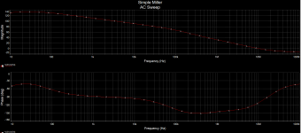
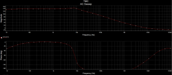
Here I achieved 140dB NFB @10KHz around output devices (Though it is still in simulation).
Here is the approach.
Normal NFB loop needs compensation to be stable. With compensation, you loose bandwidth and gain. That's major obstacle to achieve high NFB.
However, there is a way to create NFB without compensation and it is stable. That is to only include 1 or 2 components in the NFB loop.
For example, CFP output stage has local NFB. In most case, you don't need to compensate a CFP.
Another example is 2-transistor VAS in "Blameless" design. The Miller cap creates a tight local NFB, and it is stable without extra compensation.
Here is the plan. Include a push-pull class A/B output stage inside Miller compensation. In order to make it stable, inside Miller loop, you can only have 1 transistor for VAS and 1EF transistor for output.
Thus, total only 2 components inside loop, meets condition of stability without compensation.
PS: Do not use base stop resistors, base stop resistors create an extra pole.
Some overshoots may happen, even though it should be benign just like overshoots in the case of CFP.
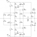
In the schematic, I also added input stage. Then, you get a CFA (Current Feedback Amp). However, if use it directly as an power amp, it lacks gain.
Thus, I configure it as unit-gain. Plan to use the whole thing as an output stage.
Before going farther, exam the open loop gain and the close loop gain.
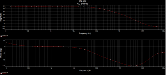
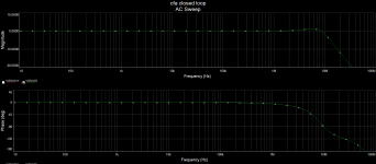
You can see, by itself, there is over 50dB NFB around the push-pull output devices.
After I put "Blameless" style input stage and vas to that "output stage".
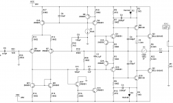
To make the entire thing stable, the outer loop ULGF must be less than the ULGF (Unit Loop Gain Frequency) of the "CFA" output stage. Choose the outer loop ULGF 500K ~ 1MHz is a safe bet.
I generated bode plots to see how much NFB around the output devices, one for simple Miller compensation and one for TMC.
PS: The bias current is around 100mA.
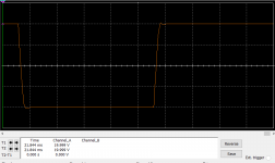
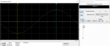
PPS: Square and Sine wave form are at 10KHz, +-20V output.
PPPS: Under tons of NFB around output devices, the remaining distortion may not come from crossover distortion. The distortion is more likely coming from input stage and VAS, because there is less NFB around input stage and VAS. I also simulated this with 0 bias case, (biased with a single diode). I can still get -90dB THD at 10KHz.
Here is the approach.
Normal NFB loop needs compensation to be stable. With compensation, you loose bandwidth and gain. That's major obstacle to achieve high NFB.
However, there is a way to create NFB without compensation and it is stable. That is to only include 1 or 2 components in the NFB loop.
For example, CFP output stage has local NFB. In most case, you don't need to compensate a CFP.
Another example is 2-transistor VAS in "Blameless" design. The Miller cap creates a tight local NFB, and it is stable without extra compensation.
Here is the plan. Include a push-pull class A/B output stage inside Miller compensation. In order to make it stable, inside Miller loop, you can only have 1 transistor for VAS and 1EF transistor for output.
Thus, total only 2 components inside loop, meets condition of stability without compensation.
PS: Do not use base stop resistors, base stop resistors create an extra pole.
Some overshoots may happen, even though it should be benign just like overshoots in the case of CFP.

In the schematic, I also added input stage. Then, you get a CFA (Current Feedback Amp). However, if use it directly as an power amp, it lacks gain.
Thus, I configure it as unit-gain. Plan to use the whole thing as an output stage.
Before going farther, exam the open loop gain and the close loop gain.


You can see, by itself, there is over 50dB NFB around the push-pull output devices.
After I put "Blameless" style input stage and vas to that "output stage".

To make the entire thing stable, the outer loop ULGF must be less than the ULGF (Unit Loop Gain Frequency) of the "CFA" output stage. Choose the outer loop ULGF 500K ~ 1MHz is a safe bet.
I generated bode plots to see how much NFB around the output devices, one for simple Miller compensation and one for TMC.


PS: The bias current is around 100mA.
PPS: Square and Sine wave form are at 10KHz, +-20V output.
PPPS: Under tons of NFB around output devices, the remaining distortion may not come from crossover distortion. The distortion is more likely coming from input stage and VAS, because there is less NFB around input stage and VAS. I also simulated this with 0 bias case, (biased with a single diode). I can still get -90dB THD at 10KHz.
Last edited:
I've had a play with this and can determine there's a good amount of current gain on the non-inverting input node, I get 120dB or so. But I can't see how this is really helping as the feedback isn't using that open loop current gain, its using the open loop voltage gain which I get to be about 54dB.
I see the input impedance is up in the megaohm region which is nice, far higher than typical VAS impedances, so I think all that extra current gain is really doing is loading the VAS much more lightly than most OS's, but that this probably isn't providing benefit.
However I think the topology does combine the local feedback benefits of a CFP stage with the fast switch-off capabilities of an EF output stage - the power devices' bases can be back-driven to speed up switch-off, unlike with CFP. It does seem to extend performance well up to 10kHz and 30kHz.
And it makes a nice stand-alone circuit unit with single high impedance input - a high voltage high power buffer.
The CFA portion implements “Output Inclusive Miller Compensation”. Configured as unit gain. Essentially all the NFB is applied on the power transistors. As you found, there is at least 50dB NFB. This amount NFB is greater than the NFB of an average “Blameless” style amp @10KHz.
However, when use it standalone, you need to use some of the gain for voltage amplification. For example, 23bB voltage gain. Then, you only left about 30bB to NFB. It can be done, but the performance will not be optimal.
However, when use it standalone, you need to use some of the gain for voltage amplification. For example, 23bB voltage gain. Then, you only left about 30bB to NFB. It can be done, but the performance will not be optimal.
Last edited:
The CFA portion implements “Output Inclusive Miller Compensation”. Configured as unit gain. Essentially all the NFB is applied on the power transistors. As you found, there is at least 50dB NFB. This amount NFB is greater than the NFB of an average “Blameless” style amp @10KHz.
However, when use it standalone, you need to use some of the gain for voltage amplification. For example, 23bB voltage gain. Then, you only left about 30bB to NFB. It can be done, but the performance will not be optimal.
Sorry, the above analysis was not correct.
For current feedback amplifier, the loop gain does not change with the ratio of the feedback resistors. The loop gain depends on the single resistor connecting between invert input and the output.
I just did some simulation. It is easy to get 10 times voltage gain out of it.
The THD is around 0.1%@10KHz.
It opens up couple of use cases. It could be a high performance output stage with GAIN. You can use common opamp to drive it from power rails with lower voltage.
Last edited:
I have already built and measured such a topology. (4 variants, the last one is combined with class-g)
The output runs at 3mA/pair at idle.
LeXaN v1 - Google Photos
The output runs at 3mA/pair at idle.
LeXaN v1 - Google Photos
I have already built and measured such a topology. (4 variants, the last one is combined with class-g)
The output runs at 3mA/pair at idle.
LeXaN v1 - Google Photos
Yep, the same output topology.
I prefer long tail pair input for outer loop to avoid DC offset issue.
Life is busy. It may take me years to build this. Do you have any store links? Or you can PM the links.