Hello diy'ers,
I've build two crecende ME amplifiers. In the last few months, I had many problems with these amps, oscillation and stuff.
I rebuild them a few times on totaly different pcb's, other components, etc.
The last version work good for about 2weeks. Than suddenly, one channel was heatig up very fast. I measured the biascurrent, it was 3amps
I turned the bias pot to decrease the current, but the bias current stays the same??
IMO, there was heavy oscillation that destroyed my 4 FET's.
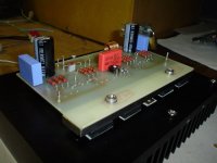
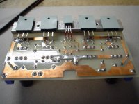
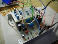
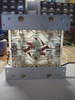
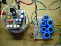
I added a few pic's. Maybe you can see any changes I have to make to minimalize the problem of oscillation.
Greets
Ben
I've build two crecende ME amplifiers. In the last few months, I had many problems with these amps, oscillation and stuff.
I rebuild them a few times on totaly different pcb's, other components, etc.
The last version work good for about 2weeks. Than suddenly, one channel was heatig up very fast. I measured the biascurrent, it was 3amps
I turned the bias pot to decrease the current, but the bias current stays the same??
IMO, there was heavy oscillation that destroyed my 4 FET's.
I added a few pic's. Maybe you can see any changes I have to make to minimalize the problem of oscillation.
Greets
Ben
Attachments
The older crescendo´s seem to oscillate when using wirewound resistors on output but the newer ME is not that sensible.
I´m even using a wirewound with the ME and don´t have any problems.
You might wanna have a look here .
See Samuels post.
At the time I built mine I had email-comtact with wuffwaff as he built quite a few of those. You might try to drop him a mail.
I´m even using a wirewound with the ME and don´t have any problems.
You might wanna have a look here .
See Samuels post.
At the time I built mine I had email-comtact with wuffwaff as he built quite a few of those. You might try to drop him a mail.
The meaning off these caps is to equalise the input capacity between de P and N FET's. I didn't do that on my original Crescendo which I build also with much less problems as the crescendo ME. If I'm not mistaking.
What I can try is to put the Zobel network after the output inductor?
When you see the back off my PCB's, I have many empty spaces. Now, if I fill these spaces up with ground plane, should this improve the stability??
I use long (20cm) wires between the PCB with the input stage and the PCB with the output devices, is this maybe also a thing I should consider to be a cause off oscilation?
Thanks
Your problem is probably in too long all wires, mainly in gate circuits. Mosfet can oscilate very easy on frequencyes up to several hundred megaherz, so you can't see it easy on scope. Try to give there litte bit higher value of serial resistor in gate. You can also give directly on gate pin an ferite pearl.
Hi Benson,
Can you post a circuit diagram?
Just by Looking at the Pics - it seems you have the input / driver stage some distance from the output stage devices - if this is the case then it implies long connections to the MOSFET Gate pins from the driver stage. Long Gate connections will result in inductance on the Gate connections - which when combined with the internal Gate capacitances of the MOSFET’s will form a Colpitts oscillator - destroying the OPS devices.
Solve by making the Gate connections as short as possible from the driver PCB & add say 10 Ohms to 50 Ohms Gate series resistors ON EACH MOSFET GATE - Add resistors as close as possible to each Gate lead - so lift each Gate lead and add between Gate lead on Mosfet and PCB - trim the Gate lead close to the MOSFET say 5mm and insert series Gate resistor - this should solve the problem - good luck.
John
I would say the same thing. Pcb design here is very critical. I had similar problems with my two first Crescendos. Then I learned how the pcb's should look like.Upupa Epops said:Your problem is probably in too long all wires, mainly in gate circuits. Mosfet can oscilate very easy on frequencyes up to several hundred megaherz, so you can't see it easy on scope. Try to give there litte bit higher value of serial resistor in gate. You can also give directly on gate pin an ferite pearl.
One critical spot is the lenght from the VAS to the mosfet. 500-1000 pF capacitances in the mosfet's together with nH's in wires creates unstableness.
If it's possible, use one pcb. Avoid wires with additional inductance and with function as antennas.
My latest attemt can be seen here:
http://home5.swipnet.se/~w-50719/hifi/qro/prototype_qro.html
http://home5.swipnet.se/~w-50719/hifi/qro/index.html
Thanks guy's for the great info,
Upupa and Peranders:
Thanks for that great links. BTW, there is now hear on my head thinking of building such a difficult amp (for me) as the DPA386. But it looks great.
JohnW:
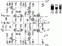
I attached a circuit diagram of de crescendo ME. And yes there is some distance between the VAS and the output devices. The gates have already 220ohm resistors. And I have already these gate resistors as close as possible to the output devices.
=> So, I'll start as soon *** possible with redrawing this PCB.
Thanks again
Upupa and Peranders:
Thanks for that great links. BTW, there is now hear on my head thinking of building such a difficult amp (for me) as the DPA386. But it looks great.
JohnW:
I attached a circuit diagram of de crescendo ME. And yes there is some distance between the VAS and the output devices. The gates have already 220ohm resistors. And I have already these gate resistors as close as possible to the output devices.
=> So, I'll start as soon *** possible with redrawing this PCB.
Thanks again
Attachments
 .
.Benson,
I had a closer look at the underside picture of your OPS board, although you have the 220R Gate resistors as close as possible on the PCB – there’s at least 1cm Lead length from the PCB to the body of the FET. If your still feeling brave – and want to give it one more try before you re-lay the PCB, try adding the Gate resistor right on the Gate pin on the device package – if you still have a problem then I would be very surprised if the issue was purely down to the VAS / Gate lead lengths. I would also look into the HF decoupling on the PSU rails – try a Ceramic decoupling capacitor (say 100N 200V) directly across the + & - PSU connections on the Drains of the Output MOSFET’s.
John
- Status
- This old topic is closed. If you want to reopen this topic, contact a moderator using the "Report Post" button.
- Home
- Amplifiers
- Solid State
- I'm going crazy, please help, Pic's