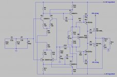
What's the opinion on the input resistor R12 being on LHS of R7 and not RHS.
We know that R7 = R16.
But in this connection does the base see R7 +R12, 16.5k to ground, instead of 15k. Or am I reading this wrong.
My question is on DC bias and not if the input filters work as drawn. Offcourse they do.
We know that R7 = R16.
But in this connection does the base see R7 +R12, 16.5k to ground, instead of 15k. Or am I reading this wrong.
My question is on DC bias and not if the input filters work as drawn. Offcourse they do.
R5 and R9 should at least go to some simple 2Q CCS's.
Then , you could just trim one CCS to get offset.
It would have 10 or more DB better PSRR (even with regulated 45v supplies).
All the fuss and bother with 2 supplies. Just derive a rail -2V (cap multiplier)
for the LTP/VAS and use those 2Q's. -90ish DB 20-20K.
OS
Then , you could just trim one CCS to get offset.
It would have 10 or more DB better PSRR (even with regulated 45v supplies).
All the fuss and bother with 2 supplies. Just derive a rail -2V (cap multiplier)
for the LTP/VAS and use those 2Q's. -90ish DB 20-20K.
OS
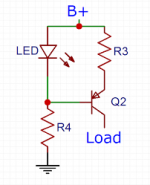
Not *necessary* because it´s a low impedance voltage source, but it does not hurt either and may reduce any residual noise.does the led need a bypass cap?
Use classic 100uF there.
Again not *necessary* because a "constant current" source has "infinite impedance" , no puny resistor will change that he he, BUT it may drop some voltage so Transistor dissipates less and receives less voltage; to boot if transistor shorts resistor still limits current to safe levels.other designs make the connection via a resistor
Choose value so it drops 1/2 to 1/3 the available voltage.
I would make R12 = 47 kΩ and R24 = 470 kΩ. Then control for offset either with a trimpot or a DC servo.
I'd be careful with the 10 pF across the MJE340/350 CB junctions.
The resistors in the bias spreader (Vbe multiplier) seem very high. That'll probably define the noise performance of the circuit. If you haven't already, simulate the performance of the biasing circuit across temperature. I'd run a DC sweep with the temperature being the controlled variable.
Have you simulated the open loop response of this circuit or are you planning to figure out the stability by trial and error? Each approach has merits. I'm just inviting you to ponder that if you haven't already.
Aside from those comments the circuit looks pretty plain vanilla. I see no reason it can't be made to work. I'm a bit curious about the connections to Q5 and Q9 collectors, though. Why not keep the input stage balanced and suckle off a little drive current for Q1 and Q3. I've seen it done with Q1 and Q3 being MOSFETs as well as they'd present an even lighter load on the input stage.
Tom
Last edited:
some replies to the above posts:
output dc offset: with the values shown the offset of the built cct is around 1mV
vbe bias cct: values choosen for 1/10th of vas I (the FETs bias is very stable)
the connections to Q5 and Q9 collectors: LTspice sims give a slight THD20 improvement, in the built cct clipping is improved with this setup
R25 is a preset in the built cct
For me, the advantage is being able to use something from the bc5xx range. Nice current gain and fairly fast for a driver. Move the disapation and voltage drop to a resistor and your choice of transistors opens up. Lower voltage offerings become viable.
Bootstrapping the driver collectors also limits the voltage that can be applied to the gates by design if you set the bootstrap voltage to around 12-15v. The zeners at the gates are just belt and braces protection. Not primary. Also, the zeners only have to work hard enough to collapse the bootstrap.
Bootstrapping the driver collectors also limits the voltage that can be applied to the gates by design if you set the bootstrap voltage to around 12-15v. The zeners at the gates are just belt and braces protection. Not primary. Also, the zeners only have to work hard enough to collapse the bootstrap.
Last edited:
why are Q5 and 9 connected to the 100R and not to the rail?
Doesn't this cost feedback bandwidth?
what is feedback bandwidth?
does it have correlation with the amps HF -3dB frequency point?
- Home
- Amplifiers
- Solid State
- before i start a pcb, any comments?