If I were you I would of checked the flatness of the device before you do the polishing. Second of all proper lapping of a soft metal like copper is extremely difficult and require counter intuitive tricks. By the pictures you have had ruined rather flat surface. In some instances to-247 flatness is given. It's around 20 micron per 100 mm / less than 1 mil over 4".I am working on a hiraga 30w amp, it has an iddle at 1.65 amps and produces alot of heat, I was not happy about die temperature versus heatsink temperature.
SKIPPED
Anybody else tried this approach?
Please check cpu lapping videos to get the idea.
Very good explanation jneutron, and I will try on my next project which is a pass amp, your method with copper and graphite.
An idea, the device shown is clean smooth copper, could one not simply solder a 2 by 2 inch copper plate with smd solder paste and then reflow the whole thing?
The reason I want a datalogger is to be able to verify the improvements from this method, it produces nice graphs or spreadsheets
An idea, the device shown is clean smooth copper, could one not simply solder a 2 by 2 inch copper plate with smd solder paste and then reflow the whole thing?
The reason I want a datalogger is to be able to verify the improvements from this method, it produces nice graphs or spreadsheets
A good method for checking flatness? Yes picture shows schratches, I could quickly see the device needed alot of work , so to speed up process I applied more pressure, then later eased of, and in the end almost no pressure.
But I will check the computer forums for further ideas
But I will check the computer forums for further ideas
I used to spray paste, but I follow silpad evolution... and experience of others.
a link for design guide:
http://www.farnell.com/datasheets/99609.pdf
a link for design guide:
http://www.farnell.com/datasheets/99609.pdf
Very good explanation jneutron, and I will try on my next project which is a pass amp, your method with copper and graphite.
An idea, the device shown is clean smooth copper, could one not simply solder a 2 by 2 inch copper plate with smd solder paste and then reflow the whole thing?
The reason I want a datalogger is to be able to verify the improvements from this method, it produces nice graphs or spreadsheets
The overmolded plastic can be damaged by soldering heat. One of the last steps in the stamping process is to form mechanical features which will hold the plastic in place. For example, the plastic edge on the bottom of the device is actually a mechanical lock, the edge of the copper has a taper and is wider at the top so acts like a key. Heating the entire bottom to 250 plus C can compromise that function.
Should the mechanical bond between the plastic and the copper be compromised, flux can wick into the device. The semi and bond wires in the past were covered with "glob top" to protect the semi and wires from the injection molding plastic process and the.different thermal expansion coefficient of the overmolded plastic. But I've been out of that industry for 30 years now, so am not sure if they just use a better overmold formulation.
Alexberg... while the spec may be very good, the actual product out there is not that good. Next time I go into work, I will look for one of the failed units, take it home and trammel it. I have dro's on my mill and a dial indicator good to go, I'll just have to 3D print a holder to lock the indicator in the R8 collet. Since I can't perfectly align the backside, I will take data every mm or so, then do a trendline fit on excel to see how it curves.
My check at work was to use a straight edge and backlight, but I will agree that is a great test of flatness with absolutely no calibration of actual curve.
Data works for me, I will try. May take a week or so.
Jn
Ps.. amplidude, unbelievably, graphene is a hugely thermally conductive material, far far better than solder. Also, using SMT paste and flux guarantees bubbles under the device due to outgassing while reflowing. In the device, they will usually stamp the copper bonding surface with a pattern of grooves who's sole purpose is to allow the outgassing a path to exit under the die.
PPS. When I wrote the thermal article for Linear Audio, I researched the junction to case values (more specifically, case to heatsink)for a large part of the IR mosfet line. They tended to use a single value for a wide variety of die size. That indicates to me that they do not use the 45 degree spread model, but are assuming the backside is being used isothermally and that it is the area of the backside used in the calculation. The reason to do that is to safely accommodate lack of flatness as well as inconsistency in mounting force.
Last edited:
I will be looking forward to your findings, and study heat transfer more indeepth.
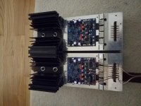
So I got both channels mechanically assembled, a process that could have taken few hours, have now stretched over several days due to lapping and polishing all heat transfer surfaces, but I'm confident it was worthwhile, and its lifespan is prolonged.
Thanks guys for all the technical insights
So I got both channels mechanically assembled, a process that could have taken few hours, have now stretched over several days due to lapping and polishing all heat transfer surfaces, but I'm confident it was worthwhile, and its lifespan is prolonged.
Thanks guys for all the technical insights
Attachments
Just finished the design in openscad, going to print it now, s/b about 2.5 hours.
Going to try using an embedment nut, so have to make an adapter for my soldering iron in brass on the lathe. Hopefully, my first try at embedment goes perfectly..
I do have some 254's in parts, so may have to trammel some.
Jn
Going to try using an embedment nut, so have to make an adapter for my soldering iron in brass on the lathe. Hopefully, my first try at embedment goes perfectly..
I do have some 254's in parts, so may have to trammel some.
Jn
my 3D printed trammel fixture worked well. I did have to chase two holes a bit, the software recently updated and I lost the compensations for internal hole size, about 400 microns too small, no problem.
I had a batch of to-254's, IRFP-250 mosfets, from the time dinosaurs roamed the planet.
Flat. totally flat to within .001 inch throughout the copper surface. The package encapsulation epoxy was almost .002 thicker on one edge than the other, but absolutely of no concern.
I will look for those non flat parts Monday at work.
jn
From: eng-tips.com:
Millipede - a thousand footed bug
Millenium - a thousand years
Million (perhaps) - a thousand thousands?
Grazie mille - a thousand thanks
The possible incongruity of "million" aside, "milli" means thousand, or thousandth.
BTW, where I work, when I refer to a "mill" instead of "a thousandth (of an inch)", people look at me as if I have two heads. This might be a peculiar "linguistic island", but my point is that mil is not universal.
It gets interesting on a multi language forum.
Here are my daffynitions..googled
mil 1 (mĭl) n. 1. A unit of length equal to one thousandth (10-3) of an inch (0.0254 millimeter), used, for example, to specify the diameter of wire or the thickness of materials sold in sheets.
mill:: a machine that manufactures by the continuous repetition of some simple action
(course, by that definition, I could also be a mill, as I "by continuous repetition of a simple action")..... make a fool of myself..")
jn
Here are my daffynitions..googled
mil 1 (mĭl) n. 1. A unit of length equal to one thousandth (10-3) of an inch (0.0254 millimeter), used, for example, to specify the diameter of wire or the thickness of materials sold in sheets.
mill:: a machine that manufactures by the continuous repetition of some simple action
(course, by that definition, I could also be a mill, as I "by continuous repetition of a simple action")..... make a fool of myself..
jn
Don't get me wrong- I think some of these amps are beautifully crafted, true works of art and craftsmanship. As a mechanical engineer/machinist, I'm wondering whether lapping the surface between the electronic device and the heatsink really makes a measurable difference in heat transferred?
No, it doesn't make any difference in the amount of heat transferred. That will be defined by the semiconductor's voltage and current, the total power dissipation. (note that for a diode, the vf will go down roughly 1 mV per degree C, so it bends the dissipation/derating curve a tad.)
What it does do is change the thermal resistance at the interface. If you dissipate 100 watts, and the thermal resistance is .5 degrees per watt, there will be a 50 degree difference across the interface. If you can get it down to .1 degree C per watt, there will be a 10 degree C difference.
Semiconductor lifetime halves every 10 degrees C.
Found my linear audio copy...
Dissipating 100 watts:
For a .5 inch by .5 inch interface, a .002 inch thick silicone grease interface will have .16 Deg C per watt, interface rise of 16 degrees C.
For a .5 inch by .5 inch mica .003 inches thick with .002 inch grease on both sides, the total is .96 degrees C per watt, interface rise of 96 degrees C.
The impact the thermal path has on semiconductor temperature and lifetime can be huge.
jn
Has anyone measured a temperature difference between lapped and unlapped transistors and heat transfer? Does it make an audible difference?
Yes, burnt out transistors dont sound good.
We're both saying the same thing, just differently.
The heat transfer mechanism can be via conduction, convection or radiation.
During conduction, the vibration amplitudes of the atoms and electrons of the metal (the heatsink and metal backing on the electronic device) become relatively large with the high temperature of the environment. Increased vibrational amplitudes (and thus the energy associated) pass from atom to atom during collisions between the atoms.
One of the laws of thermodynamics is that heat is always transferred from hot heat to cold. Call it a system, a reservoir. It's called a law because this is validated through experimentation and heat always goes from hot to cold. This happens through experimentation every time. No exceptions.
Experiments show the conduction rate P (amount of energy transferred per unit time) is:
P=Q/t = k/A[(Thot - Tcold)/(L)]
Where:
k is the thermal conductivity of the material
Q is the energy that is transferred as heat through material from it's hot area to cold area per unit of time
t is time
L is the thickness of the conducting material, in this case thermal paste
My entire point is that conduction rate P is inversely proportional to L. Thermal paste is added to aid heat conduction between the electronic device and the heatsink. Less heat equals more life for the electronic devices.
Is it worth the time and effort to lap the transistors? If so, what difference does it make? Do the transistors last many years longer?
Last edited:
Thermal paste is a dismally poor conductor of heat.
The only reason for thermal paste is to fill the gaps in the surface roughness, be it 200 microinch or 500.
The proper application of thermal paste is to simply put some on the surface and scrape it all off using the edge of a single edge razor. It should only fill the gaps.
Everybody goops it on, and uses the screw pressure to squeeze out the excess. Very bad technique, not how paste was designed to be used. For the .5 by .5 inch example I detailed, it's .08 degrees C per watt per .001 inch thickness.
Lapping the surfaces and then using just a film of paste will give the absolute best thermal transfer, the only thing better is a sheet of graphene used between a heat spreader and the case, using the thickness of the heat spreader to gain conductive area.
BTW, you included area (A) in the equation, but didn't mention it. If the package bottom is concave, the effective area no longer includes the middle of the bottom which is exactly where the die is located.
10 degrees C rise, half the life. Arrhenius equation. Used in MTBF calculations for large systems. And do NOT ask me about MTBF...That is a chapter in my life that I want to forget... (had to put together an MTBF presentation for very high level people for a 10e9 dollar machine, at the last minute they changed the presentation date but I was in Colorado on vacation. A person who used to be my friend gave the presentation. Now, he tries to run me over in the parking lot every chance he gets.)
But more importantly, many solid state circuits do not play well when the die gets hot. Bipolars change gain, bias points change, cooler is always better. The thermal time constant of a bipolar junction is 100 uSec to 1 mSec, but the thermal constant to the exterior of the case is the 1 to 5 second regime, and can be even longer if the thermal transfer is bad and there is any heatsink mass.. If your thermal tracking sensor for bias is on the heatsink and the die dissipates heavily, your sensor can be tens of degrees too low, that can cause runaway.
jn
The only reason for thermal paste is to fill the gaps in the surface roughness, be it 200 microinch or 500.
The proper application of thermal paste is to simply put some on the surface and scrape it all off using the edge of a single edge razor. It should only fill the gaps.
Everybody goops it on, and uses the screw pressure to squeeze out the excess. Very bad technique, not how paste was designed to be used. For the .5 by .5 inch example I detailed, it's .08 degrees C per watt per .001 inch thickness.
Lapping the surfaces and then using just a film of paste will give the absolute best thermal transfer, the only thing better is a sheet of graphene used between a heat spreader and the case, using the thickness of the heat spreader to gain conductive area.
BTW, you included area (A) in the equation, but didn't mention it. If the package bottom is concave, the effective area no longer includes the middle of the bottom which is exactly where the die is located.
10 degrees C rise, half the life. Arrhenius equation. Used in MTBF calculations for large systems. And do NOT ask me about MTBF...That is a chapter in my life that I want to forget...
(had to put together an MTBF presentation for very high level people for a 10e9 dollar machine, at the last minute they changed the presentation date but I was in Colorado on vacation. A person who used to be my friend gave the presentation. Now, he tries to run me over in the parking lot every chance he gets.)But more importantly, many solid state circuits do not play well when the die gets hot. Bipolars change gain, bias points change, cooler is always better. The thermal time constant of a bipolar junction is 100 uSec to 1 mSec, but the thermal constant to the exterior of the case is the 1 to 5 second regime, and can be even longer if the thermal transfer is bad and there is any heatsink mass.. If your thermal tracking sensor for bias is on the heatsink and the die dissipates heavily, your sensor can be tens of degrees too low, that can cause runaway.
jn
Last edited:
We're both saying the same thing, just differently.
The heat transfer mechanism can be via conduction, convection or radiation.
During conduction, the vibration amplitudes of the atoms and electrons of the metal (the heatsink and metal backing on the electronic device) become relatively large with the high temperature of the environment. Increased vibrational amplitudes (and thus the energy associated) pass from atom to atom during collisions between the atoms.
One of the laws of thermodynamics is that heat is always transferred from hot heat to cold. Call it a system, a reservoir. It's called a law because this is validated through experimentation and heat always goes from hot to cold. This happens through experimentation every time. No exceptions.
Experiments show the conduction rate P (amount of energy transferred per unit time) is:
P=Q/t = k/A[(Thot - Tcold)/(L)]
Where:
k is the thermal conductivity of the material
Q is the energy that is transferred as heat through material from it's hot area to cold area per unit of time
t is time
L is the thickness of the conducting material, in this case thermal paste
A is face area
My entire point is that conduction rate P is inversely proportional to L. Thermal paste is added to aid heat conduction between the electronic device and the heatsink. Less heat equals more life for the electronic devices.
Is it worth the time and effort to lap the transistors? If so, what difference does it make? Do the transistors last many years longer?
- Status
- This old topic is closed. If you want to reopen this topic, contact a moderator using the "Report Post" button.
- Home
- Amplifiers
- Solid State
- Transistor heat transfer capability