Hi everyone,
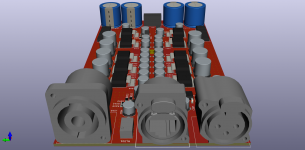
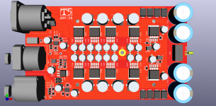
I just (hopefully) finished the PCB layout for our LPUHP clone. The board hosts XLR input, RJ45 power-good/mute connections and speakON output connections and is intended to be used in this case: F 1048-160 KWL | BOPLA
Board setup is 4 layer with signal/GND on top, GND on layer 2, +/-18V on layers 3 and 4.
We added supply under/overvoltage monitoring which will be communicated back to our controller, a mute relay driven by the controller and also a DC servo.
The feedback for the noninverting branch of the difference amplifier (U202A) is taken directly from the GND-output pin of the speakON connector to make it ignore possible ground bounce in the groundplane induced by currents flowing towards the output connector.
I'm looking forward to any comments regarding routing and placement, especially regarding the last point mentioned.
Attached please find the schematic as PDF, copper layers 1-4 as PDF and 3d renderings.
Cheers, Jürgen
Edit: A small note about cooling: The PCB will be mounted up side down in the case with a aluminium plate abt. 3x93x100mm and a silicone pad under all the DPAK packages for heat transfer to the top side of the case.
Attachments
Last edited:
Btw. if someone wants to look at the kicad source files, here they are: Jurgen Herrmann / AMP-DR * GitLab
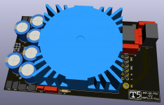
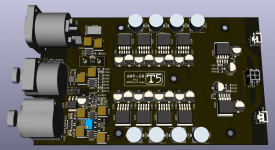
There has been progress v1 was built, extensively tested and modified.
v2 has been designed, built and measured also. measurements will be posted soon...
Here are the urls to the gitlab repos:
Jurgen Herrmann / AMP-DR * GitLab
Jurgen Herrmann / AMP-DR-PSU * GitLab
Schematics, layouts and renderings in the attachments.
v2 has been designed, built and measured also. measurements will be posted soon...
Here are the urls to the gitlab repos:
Jurgen Herrmann / AMP-DR * GitLab
Jurgen Herrmann / AMP-DR-PSU * GitLab
Schematics, layouts and renderings in the attachments.
Attachments
Last edited:
Hi Jürgen,
just a few ideas to consider, as inspiration not criticism:
Adding small resistors in series with the output of each parallel LME49600 to ensure load sharing?
Pin one of the XLR connector connected to chassis? - Yes
Small capacitors or R-C snubbers across the PSU rectifier diodes?
R-C snubber across the transformer secondaries to tame resonance?
Adding some small inductor or resistor between the PSU filter caps forms a low-pass filter improving high frequency PSRR where the regulators PSRR start to decrease. If you have space, you can build low value resistors on the PCB free of charge.
You have different capacitors parallel in the PSU. Have you checked for parallel resonance between the caps?
Why did you reduce the capacitance at the regulators input?
Overall, impressive design, well done.
Edit: Sorry I didn't notice the schematic was updated.
Servus,
Lee
Last edited:
Adding small resistors in series with the output of each parallel LME49600 to ensure load sharing?
This has proven not to be a problem, as in the original design. So they were omitted. The LME49600 has a pretty high output impedance (open loop) anyways.
Pin one of the XLR connector connected to chassis?
R-C snubber across the transformer secondaries to tame resonance?
Look more closely... 😀
The above has been implemented. Pin1/Shield of XLR connected to chassis as stated in the schematics.
Adding some small inductor or resistor between the PSU filter caps forms a low-pass filter improving high frequency PSRR where the regulators PSRR start to decrease. If you have space, you can build low value resistors on the PCB free of charge.
I'd guess there is enough attenuation of HF stuff by the input filter and by the RC snubber on the transformer. Additionally there is some trace resistance and the lead resistance from the psu board to the amp board. I crudely checked EMI immunity by holding a phone thats transmitting right next to the PCB. No changes in measurements (f.ex. multitone) were detected. Seems pretty immune to EMI to me so far.
You have different capacitors parallel in the PSU. Have you checked for parallel resonance between the caps?
Lee
No, that's actually something I cannot reasonably check. At least there's no method I know of to measure such things. Do you know one?
Last edited:
Servus Jürgen,
you were faster answering than me revising my post. I also overlooked you built it already. Do you have some photos of the build?
Yes, pin one is connected properly in the second schematic.
The suggestion for the load sharing resistors stems from recommendations paralleling OP amps and you're right this might not be needed with those buffers and their high output impedance.
A cell phone is a good way to check EMI resistance. In case there was no influence, immunity is proven in practice.
I don't know a way to check for parallel resonance, other than trying to simulate it based on assumed component and wiring inductance and resistance. My observation simulating this is that the result may be surprising sometimes.
Regarding the simulation of the parallel caps - I just gave up on the idea as we use two mostly undisturbed power planes for +/-18V (It's a four layer board) and the calculation of the inductances of the planes are beyond my capabilities. Also whipping up a simulation model with all the different inductances between all the caps is more than tedious and I doubt it will bring any meaningful insight. I'm open to suggestions though!
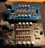
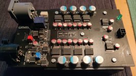
As for the pics, here you go. The blue one is v1, the black one is v2.
As for the pics, here you go. The blue one is v1, the black one is v2.
Attachments
The PCBs and assembly look great!
Do you solder by hand or improvise some reflow process?
If I see correctly, you are paralleling electrolytic caps with ceramics, which usually isn't an issue anyway.
Agree, it is super difficult to predict the PDN when using planes. On the other hand, it is less likely to have issues when using planes. Looks alright.
We are using a pizza oven to do the reflow soldering. The temperature profile is controlled by a multimeter with temperature probe and usb interface, a small python script and a usb-controlled solid state relay. Ramp up to 90°C with 1500W, soak to 150°C with 675W, then reflow till 225°C are reached with 1500W. Very hacked-together but with fresh solder paste (leaded) it works just beautifully now. I'd call the result "perfect"!
Those black "boxes" are actually WIMA PPS foil caps. No ceramics allowed near anything in the audio path. And the PSU is in the audio path IMHO 🙂
EDIT: Except those small EMI suppression caps - those are C0G ceramics.
Those black "boxes" are actually WIMA PPS foil caps. No ceramics allowed near anything in the audio path. And the PSU is in the audio path IMHO 🙂
EDIT: Except those small EMI suppression caps - those are C0G ceramics.

- Home
- Amplifiers
- Solid State
- Comments on PCB layout for LPUHP clone wanted