Hello friends, this is the story.
A good friend enjoyed this amplifier for about 10 years until one channel exploded. This also killed one of his favorite and expensive speakers. He asked me to take a look at it and try to fix it.
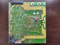
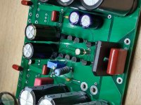
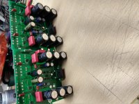
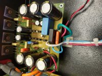
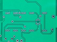
It has 2 identical small PCB's, one still works, the other can't be fixed because it caught fire. Literally. You may like to see the uploaded pictures.
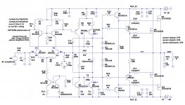
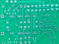
I made some research and could disassembly the dead channel PCB, and could entirely personally redraw the PCB and have it manufactured. The entire schematic could be deduced from the bare PCB. All parts measured. I am also uploading the schematic. The LTSpice working simulation file is also provided. I could recognize this circuit as some Goldmund variant, probably model 330. I tried making some of these variants from information gathered from this same site and I could make them work almost with no problem. The circuits I used were simpler, with Semelabs BUZ900/905 MOSFETS, and a simpler driver stage.
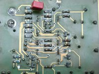
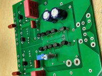
You can clearly see the different color of the PCB soldering mask. Lighter green for the old original amplifier, and darker green for my new, copied PCB. I bought all the parts from Mouser except for the lateral MOSFET's that I replaced for Exicon parts, obtained from Profusion, GB.
The problem: being the new PCB's identical to the originals, and being the original working board fairly stable and well behaved, the new replacement boards (I made 2 of them) is making me nuts 😱. The working voltage is +/- 60V and when my variac reaches the point for +/- 40V, I get a strong 22 MHz sine oscillation at the speaker output (no load), input shorted.
All kind of solutions I tried with no reasonable results at all. The only difference are the output MOSFETS. EXC10N20 and ECX10P20 in place of the originals Hitachi famous 2SK1058 / 2SJ162.
Ferrite bead on the gate terminal of each MOSFET, larger stopper gate resistors, small Zobel network placed across drain to gate of each MOSFET, compensation capacitors at previous VAS stage, heat sink connected to ground, etcetera.
Some strange things I detected by testing the original working amplifier.
In some way I think I could understand the reason, later on.
The working amplifier does not show quiescent current of the output MOSFET's. The offset balance trimpot does not show any kind of output DC change at the output when adjusted. The attached schematic shows this trimpot as R3 and R4. The output DC voltage with input shorted is about 2 mV or less. When applying input signal to this working amp, it shows no visible distortion, and delivers full 55 Vp-p sine wave from 5 to 50 KHz flat.
BTW, very hot Q1 and Q5 ! ... being small signal transistors TO-92. I believe that this could be the reason for no quiescent current at the output devices. I tried to raise Iq a little for a short time by changing R7 value from 330 to 430 Ohms. This should increase quiescent current to 130 mA per output device, that MOSFET's usually like. It worked, but Q1 and Q5 suffered. I returned to the original 330 Ohms value. But this amplifier and his twin worked for 10 years almost all day long, with excellent sound quality.
In the other hand, I don't know what else to do with my copy version. The Exicon MOSFET'S were ordered as matched units, 18 of each type N and P.
The only thing that make the oscillation stop was to place 2 x 100pF C3 and C4 capacitors, which I think is a huge value. The oscillation stopped but the output devices quickly raised their temperature, I don't understand why ! I thought I had solved the problem. 😕
Also, I lowered the feedback resistor R22 to 3K75 half its original value. No changes.😡 returned to riginal 7K5 Ohms value.
Please, could somebody help me think what can be done to make this amp work ? I would thank this help very much.
Finally: today I ordered 20 units 2SK1058/2SJ162 from Pacific Semiconductor in Canada, to avoid any fakes from other source. I have not too much hope because these are not matched units and these are too few pieces to get at least 2 matched pairs...
Thank you in advance !
A good friend enjoyed this amplifier for about 10 years until one channel exploded. This also killed one of his favorite and expensive speakers. He asked me to take a look at it and try to fix it.
It has 2 identical small PCB's, one still works, the other can't be fixed because it caught fire. Literally. You may like to see the uploaded pictures.
I made some research and could disassembly the dead channel PCB, and could entirely personally redraw the PCB and have it manufactured. The entire schematic could be deduced from the bare PCB. All parts measured. I am also uploading the schematic. The LTSpice working simulation file is also provided. I could recognize this circuit as some Goldmund variant, probably model 330. I tried making some of these variants from information gathered from this same site and I could make them work almost with no problem. The circuits I used were simpler, with Semelabs BUZ900/905 MOSFETS, and a simpler driver stage.
You can clearly see the different color of the PCB soldering mask. Lighter green for the old original amplifier, and darker green for my new, copied PCB. I bought all the parts from Mouser except for the lateral MOSFET's that I replaced for Exicon parts, obtained from Profusion, GB.
The problem: being the new PCB's identical to the originals, and being the original working board fairly stable and well behaved, the new replacement boards (I made 2 of them) is making me nuts 😱. The working voltage is +/- 60V and when my variac reaches the point for +/- 40V, I get a strong 22 MHz sine oscillation at the speaker output (no load), input shorted.
All kind of solutions I tried with no reasonable results at all. The only difference are the output MOSFETS. EXC10N20 and ECX10P20 in place of the originals Hitachi famous 2SK1058 / 2SJ162.
Ferrite bead on the gate terminal of each MOSFET, larger stopper gate resistors, small Zobel network placed across drain to gate of each MOSFET, compensation capacitors at previous VAS stage, heat sink connected to ground, etcetera.
Some strange things I detected by testing the original working amplifier.
In some way I think I could understand the reason, later on.
The working amplifier does not show quiescent current of the output MOSFET's. The offset balance trimpot does not show any kind of output DC change at the output when adjusted. The attached schematic shows this trimpot as R3 and R4. The output DC voltage with input shorted is about 2 mV or less. When applying input signal to this working amp, it shows no visible distortion, and delivers full 55 Vp-p sine wave from 5 to 50 KHz flat.
BTW, very hot Q1 and Q5 ! ... being small signal transistors TO-92. I believe that this could be the reason for no quiescent current at the output devices. I tried to raise Iq a little for a short time by changing R7 value from 330 to 430 Ohms. This should increase quiescent current to 130 mA per output device, that MOSFET's usually like. It worked, but Q1 and Q5 suffered. I returned to the original 330 Ohms value. But this amplifier and his twin worked for 10 years almost all day long, with excellent sound quality.
In the other hand, I don't know what else to do with my copy version. The Exicon MOSFET'S were ordered as matched units, 18 of each type N and P.
The only thing that make the oscillation stop was to place 2 x 100pF C3 and C4 capacitors, which I think is a huge value. The oscillation stopped but the output devices quickly raised their temperature, I don't understand why ! I thought I had solved the problem. 😕
Also, I lowered the feedback resistor R22 to 3K75 half its original value. No changes.😡 returned to riginal 7K5 Ohms value.
Please, could somebody help me think what can be done to make this amp work ? I would thank this help very much.
Finally: today I ordered 20 units 2SK1058/2SJ162 from Pacific Semiconductor in Canada, to avoid any fakes from other source. I have not too much hope because these are not matched units and these are too few pieces to get at least 2 matched pairs...
Thank you in advance !
Attachments
-
Sim.zip5.2 KB · Views: 163
-
 Goldmund_Clone_01.jpg980.5 KB · Views: 1,144
 -
 Goldmund_Clone_02.jpg868.2 KB · Views: 1,048
 -
 Goldmund_Clone_03.jpg754.4 KB · Views: 987
 -
 Goldmund_Clone_05.jpg652.2 KB · Views: 1,123
 -
 SimulationSchematic.jpg483.5 KB · Views: 1,289
 -
 Goldmund_Clone_10.jpg655.4 KB · Views: 924
 -
 Goldmund_Clone_09.jpg972.3 KB · Views: 476
 -
 Goldmund_Clone_original_01.jpg982.8 KB · Views: 514
Q4 and Q13 need compensation caps perhaps? Try larger C3/C4 value?
You've swapped Q2<->Q5 and Q1<->Q8, the 5551 and 5401 are the high voltage parts.
I really don't like the zener/1N4148 gate-oxide protection components not being directly on the MOSFET gates - they do not protect placed behind other components - this may account for the failure that happened.
And add fuses between filter cap and amp rails!
I have to say you did a pretty good job. 😉
I assume that oscillations in that frequency range originate from the output MOSFETs.
I designed a similar lateral MOSFET amp this year you will find documented here Just another lateral FET amp
equipped with NOS 2SK135/J50 that works with +-35V.
For me capacitors of 100~220pF directly connected to drain-gate of the power MOSFETs did the trick.
And I had to decouple the LPT and VAS supply from gate buffers otherwise I observed oscillations of 200MHz😡
Besides I assume that the loop compensating caps could be further optimized - but at a first glance this should work.
Btw I would not move the gate protecting zeners.
edit: I see blocking voltage of Q1/Q5 are not suitable for +-60V supply, use 5401/5551 instead (available in smd as well)
Last edited:
PCB-layout: I would connect the rail blocking caps the shortest way to power-gnd, but not in a loop around the driving circuit.
Btw this is the first time I see exploded lateral MOSFETs
Btw this is the first time I see exploded lateral MOSFETs
Last edited:
edit: I see blocking voltage of Q1/Q5 are not suitable for +-60V supply, use 5401/5551 instead (available in smd as well)
That's due to the swapping I mention - the left hand one's have a 10k resistor to soak up voltage. Still its probably better to match them anyway.
agreed. Btw I would prefer BJTs at the input differential pair: Lower offset (no pairing required), higher transconductance and - available.
Last edited:
I would not say wrong, but far overcompensated degrading bandwidth down at no avail.Compensation is wrong, you can't use lag compensation as high as 100pF...see attach as my quick fix, along with other changes.
Thank you Mark Tillotson, voltwide , aparatusonitus for your replies. I would like to study any single provided option and suggestion, so I will try to resume them.
Just as little remark: I am not the designer of these original amplifiers. For some reasons, I can't change or modify too much this PCB. I really think that it has many design errors, but there is a matter of physical dimensions to fit the enclosure mounting that won't allow me to make some hardware changes, such as adding heat sinks, changing transistor's packages for dissipation reasons, etc.
What I do have is the proof of an original, live, working amplifier board, so I need to fix the actual brand new missbehaved board and make it work. And my question is: what is causing such a behaviour difference when the PCB's (original and new) are mirror copies, being the MOSFETs the only change?
I mean that I can happily accept all valuable ideas and try swapping transistors, change and/or adding capacitors, change resistor values, etc. but I won't be able to make major changes, as you can understand.
Ideas to be studied and tested ( and some more questions and notes over all this)
01. Q3-Q4-Q6-Q13 need compensation ? Suggested normal values ?
02. larger C3/C4 value ? Suggested normal values ?
03. swapping Q2<->Q5 and Q1<->Q8. Agreed. Would this really their stop heating ?
04. zener/1N4148 not being directly on the MOSFET gates. I can't really change this.
05. add fuses between filter cap and amp rails. Done.
06. assume oscillations originate from output MOSFETs. I will now check output with a 350 MHz scope. I was using my 60MHz Tek
07. try 100~220pF connected to drain-gate of power MOSFETs. Would this degrade normal frequency response?
08. check for oscillations of ~200MHz. Is this causing MOSFETs heating when oscillation apparently stops increasing C3/C4?
09. optimize loop compensating caps. Please wich caps and values ?
10. connect the rail blocking caps the shortest way to power-gnd. I will study the way to do this.
11. prefer BJTs at the input differential pair. I can't change this.
12. wrong compensation and various interesting fixes (please see note below) (*)
13. amplifier far overcompensated degrading bandwidth. Up to now only C3/C4 = 100pF apparently stopped oscillation. MOSFETs get HOT !
(*) aparatusonitus: thank you for taking valuable time. I have studied your circuit, it is really interesting. Unfortunately I won't be able to make such a deep modification to the circuit in this case. Maybe I can try some of them, those that are physically and electrically possible. For example there is no room for TO-126 package transistors such as MJE340/350. Please see the details of both sides of the bare PCB. The original designer used a very tight spacing for TO-92 transistors, leads too close, and there is a "star ground plane" so it is very hard to place new components. I can just solder some components here and there or change values.
Attachments
Easiest remedy is to replace both pcb's with bought in amplifier pcb's.
Millions on ebay.
Millions on ebay.

what is causing such a behaviour difference when the PCB's (original and new) are mirror copies,
being the MOSFETs the only change?
Usually C6 would be more like 100nF.
I suspect it should be 2N5551 not 2SC5551.
Using TO-92 devices like BC546/BC556 in the VAS position is asking for trouble. Also, with the 60V rails, these devices are over their maximum Vce... probably why the original blew up!
edit: Also looks like C17 and C8 should go to ground
Using TO-92 devices like BC546/BC556 in the VAS position is asking for trouble. Also, with the 60V rails, these devices are over their maximum Vce... probably why the original blew up!
edit: Also looks like C17 and C8 should go to ground
Thank you, but I am here to learn, and it took some effort to copy the PCB by myself. I hope that with the advice of the friends here I will make the oscillation stop. Boards are identical, there must be some solution.
Thank you rayna and jaycee, I will check all this tomorrow and report. As I explained before, I have on working amp. It is the new board that fails.
Thank you rayna and jaycee, I will check all this tomorrow and report. As I explained before,
I have on working amp. It is the new board that fails.
It is easy to get a part wrong by a factor of ten, be sure all R and C are the correct values.
And do try C6 = 100nF, with an 8R dummy load.
Last edited:
Sure rayna, I will check all the values again. You are right x10 errors are common.. The Zobel cap should probably be 100n. About C17 and C18 I think that the original is connected as shown. But I will check.
before modding the caps you should set the output bias to some 100mA. I suspect the original is set close to zero which alters susceptibility to oscillations in an unknown way.
I switched to a Tektronix 2465 oscilloscope and checked if the amp was oscillating > 100~300 MHz. No HF oscillations when C17 and C8 = 100pF but the MOSFETs get hot in about 5 seconds. I am now uninstalling the 4 MOSFETs. There are no shorted parts. So I will test the voltages of several key points without the power devices. I have measured all gates +/-3V or more compared to the +/-430 mV in my simulation with input shorted. This could explain the heating without oscillation.
Many tests to do, so I will return with some interesting data. I am checking the complete schematic looking for some components value errors as rayma suggested. This bias of ~2mA is very strange. Corrected the wrong part no. 2SC5551. Just the schematic is wrong, all the boards (old and new) use 2N5551.
Also, I am now replacing BC546/BC556 for 2N5551/2N5401 as suggested. These transistors are in the limit of teit working VCEO value.
I will be back as soon as possible.
Also, I am now replacing BC546/BC556 for 2N5551/2N5401 as suggested. These transistors are in the limit of teit working VCEO value.
Please don't do that...you will go over SOA again, devices will heat up more than they can handle in the long run. You need transistors that can dissipate min. 1W, so get Zetex (aka Diodes) ZTX656/756_ZTX657/757_ZTX658/758 as they can be supplied via Mouser/Farnell. It will fit fine on pcb as they are in the TO-92 (E-line) housing and besides the pinout is the same for both types of transistors (1-C; 2-B; 3-E) ... don't be fooled by the way pinout is shown in both datasheets!!!
Hmm...i was looking at the schematic you gave so i assumed BC546/BC556 were used as VAS transistors instead of 2N5401/5551. Therefore, if 2N5401/5551 were used on the second differential, you would have to rotate the Zetex transistors by 180°.
- Home
- Amplifiers
- Solid State
- Fixing and troubleshooting this MOSFET amplifier