It seems to me that this kind of circuits aren't suitable for split power supplies, as the DC offset at the output can't be accurately fixed to 0V. Also, 1.5Ω in the emiters are too high to drive 4Ω loads, you are loosing about 40% of the output swing there.
I would try another better configuration, IMHO.
I have built the original circuit with split power supply and the DC offset at the output is very stable and I use the amplifier every day for some years now.
The emitter resistor is 0.47Ω in my new modified circuit. Maybe I have to decrease this to 0.22 Ω. I will check that.
I'm thinking... replace the output pair with lateral FET's. That would overcome the limitation of the driver stage and laterals should also be stable in bias current with the simple bias scheme this amp has.
If you really want to go dual rail then add a simple servo.
This is a nice idea. I think I will try it!
The new design has a lot of volts wasted in the current sink load using two green LEDs in series. Lose one of the LEDs and reduce the resistor accordingly perhaps? This should lead to more symmetrical clipping (which is one of the stated goals).
You have no high frequency decoupling on the PSU rails.
Nice idea! One green LED is enough.
I run the simulation with only one LED and decreasing the resistor to set the same current. This gave only 0.2 more Volt at the negative side.
But I will keep your proposal.
The circuit in question is definitely that by JLH in published in Wireless World in 1970.
At one time I had that issue in my possession. The additional diode modification to the standard quasi complementary output stage (later recast in form by Baxandall) appeared in a letter from I.M.Shaw in the same issue of that magazine.
Initially I was not attracted by the use of bootstrap connections and the unbalanced look of Linsley-Hood's circuit. This and the preceding introductory article gave rise to a series of challenging letters to the editor and the idea never caught on.
It was recently reported that the latest Rega amplifiers incorporate some of Linsley-Hood's output stage thinking so it is remarkable nearly 50 years on the thinking is not completely dead.
Linsley-Hood's original aim was to devise a circuit to rival the simple Class A circuit Hood had designed but without the penalty of the heat dissipation involved.
That is the context of my current interest since I have a 1996 Class A which has that issue. I will save my comments on the AB design for later.
The Quad 303 which succeeded the Quad II used a quasi complementary triple output stage.
I have also built a lower power version of the JLH 1996 Class A amplifier and the only problem is than runs very-very hot. Especially here in Greece it is not possible to operate it during the hot days of summer.
So I was looking for another solution and I built the original JLH Class AB (1970 circuit). It runs without much hot and I cannot hear any difference with the Class A (1996) circuit.
regards
George
This amp ran very high bias currents in both the driver and outputs, which would mean it generated a lot of heat even undriven. This was probably necessary because the compensation is a very large cap that bypasses the output out of the feedback loop so any cross-over distortion is not controlled by the feedback.
Your simulation raises the total supply voltage from 47 to 68 Volts. This is contrary to the need for operation with lower impedance loads while maintaining the thermal dissipation. However the original high bias currents mean the dissipation was much higher than it need be so if you can reduce the bias current to more typical levels then heat may not be a problem. But I have to wonder why you changed the voltage unless you plan to change the power transformer?
Experienced DIYA would completely redesign the amplifier board to a modern circuit but even they might be tempted to just buy existing modules from Apex or China/Amazon. It depends on if you just want a working solution or do you want to "make it your own".
You can reuse the power transformer for a bipolar circuit by creating a ground voltage half way between the 47V + and -, ei make 23.5V ground and float the existing negative. This takes two big ecaps instead of one.
One more thing. Bootstrapping is a great way to maximize voltage swing.
I should repeat what Mooly and Mark said: MOSFETs would be a good way to correct the lack of output current and the two LEDs is wasteful of voltage. If you choose to continue with the 100mA driver current then I would replace the LEDs with small diodes (~1n4148) and replace the emitter resistor with about 6.8 Ohms. Using MOSFET outputs, 25mA driver current would be plenty.
As I mentioned in post #1, I used split power supply even for the original circuit of JLH 1970 amplifier.
Also I want to keep the original amplifier, and I want to built a new one with the suggested modifications.
Yes, I agree it is a good idea to decrease the voltage of the power supply, for a 4 Ω load. But I have found that the maximum peak voltage that I need for my loudspeaker is about 25-26 Volt peak during loud passages of music. So that is why I use a voltage of +/- 34 Volt and accept the greater heat consumption.
I will keep only one LED for the current source.
thanks
George
I am interested in assembling this amp. I have the required semis.(current replacements). Can some one help in finalizing the design, PCBs etc ?
Also, transformer, Caps, box and Heatsinks !
I will design a PCB when the amplifier design is finalised. But this it will take some time I think!
I will post also the LTspice files later.
The amplifier at the left is the one that J. Linsley Hood describes in the Wireless World, July 1970, article. I don't think it is the Quad.
Look here
https://www.vintageshifi.com/repertoire-pdf/pdf/telecharge.php?pdf=Quad-303-Owners-Manual.pdf
You can read the original article of JLH here :
https://americanradiohistory.com/Archive-Wireless-World/70s/Wireless-World-1970-07.pdf
See page 321 of the magazine.
I see some similarities but the Quad is much more complicated.
regards
George
Another option is to add an pair or large power transistors to the existing circuit. 25 years ago, I did this to a Sansui G-4700 receiver that I was given because it had blown up. You change the existing emitter resistors to about 2 Ohms and drive the added transistors (c/w heat sink) from there. I used a 2n3773's and 2.2 Ohms. Note this was quasi addition to a complementary circuit so the lower 2n3773 was driven from the PNP collector. Depending on the bias, this gives only fair THD but indestructible output. My old receiver has since been shorted and abused with no failure. The idea is a bit like current dumping. It would be a great way to handle low-Z loads.
Dear steveu,
Can you kindly add your suggestion to the .asc file, appended below.
It turns out that D1 is a big part of the 4 Ohm problem, ie it is a current limit that kicks in even before the PNP runs out of gain. But you still need more gain on the PNP side so the best solution is to add a pnp driver and replace your big PNP with a NPN, and the emitter resistors need to be reduced.
I should note that using the big PNP as a driver with a quasi NPN added like this leads to stability problems because the big PNP is slow. Drivers need to be fast. You could also drive the big PNP with a pnp driver but then the bias needs to change etc. Lots of possibilities but this is probably the best bang-for-the-buck.
And the bias should be changed to a VBE multiplier but I didn't show that here.
And I didn't fine tune the current limit. This is related to the emitter resistor values.
Attachments
Last edited:
It turns out that D1 is a big part of the 4 Ohm problem, ie it is a current limit that kicks in even before the PNP runs out of gain.
How you came to this conclusion?
If I remove completely the zener D1 from the circuit, the simulation shows that the maximum voltage at the negative side does not increase in level.
The original JLH was class A:
J. L. Linsley Hood, "Simple Class -A Amplifier", Wireless World, April 1969.
The 1970 design is class AB
Jan
Yes.
As JLH states at the article, the 1970 class AB design was a try to achieve the good listening performance of the 1969 class A design. And according to his words from the 1970 article:
"However, the most careful comparative listening trials, with several of the author's long suffering friends, have failed to uncover any audible difference between these two designs, both of which will almost certainly surpass in performance the best available valve-operated, transformer-coupled units."
And the big advantage of the 1970 design is that it does so without the heat.
regards
George

OTon/
George, I enjoyed your recent articles in AudioXpress!
/OToff
Jan
Jan, it's always a pleasure to read kind words from you! Thank you!
Actually, I was thinking to use this amplifier to drive some of the channels of my AXL active loudspeaker.
What do you think about this? Any suggestions ? I appreciate your knowledge about amplifiers.
regards
George
It turns out that D1 is a big part of the 4 Ohm problem, ie it is a current limit that kicks in even before the PNP runs out of gain. But you still need more gain on the PNP side so the best solution is to add a pnp driver and replace your big PNP with a NPN, and the emitter resistors need to be reduced.
I should note that using the big PNP as a driver with a quasi NPN added like this leads to stability problems because the big PNP is slow. Drivers need to be fast. You could also drive the big PNP with a pnp driver but then the bias needs to change etc. Lots of possibilities but this is probably the best bang-for-the-buck.
And the bias should be changed to a VBE multiplier but I didn't show that here.
And I didn't fine tune the current limit. This is related to the emitter resistor values.
I appreciate this is has not been subject to a wide battery of tests.
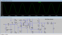
I have tried a single THD test which shows the maximum peak output voltage to be at little below 16 Volts into 4R with 20kHz sine wave input. The THD is about 0.05% provided C11 and R18 are left out -if not the figure rises to 2.6%
without D1
My guess is that you didn't change the load to 4 Ohms? Attached is two simulations with and without D1 into 4 Ohms.
How you came to this conclusion?
If I remove completely the zener D1 from the circuit, the simulation shows that the maximum voltage at the negative side does not increase in level.
My guess is that you didn't change the load to 4 Ohms? Attached is two simulations with and without D1 into 4 Ohms.
Attachments
Yes.
As JLH states at the article, the 1970 class AB design was a try to achieve the good listening performance of the 1969 class A design. And according to his words from the 1970 article:
"However, the most careful comparative listening trials, with several of the author's long suffering friends, have failed to uncover any audible difference between these two designs, both of which will almost certainly surpass in performance the best available valve-operated, transformer-coupled units."
And the big advantage of the 1970 design is that it does so without the heat.
regards
George
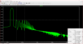
The piece you have quoted attracted my interest too. One might expect if such is the case then the FFT of the Class AB design would resemble that for the Class A.
The closest I have been able to get to this is with any simulation is for the second to fourth harmonics to decline in a uniform pattern.
For this result the output Iq has somewhat of a sweet spot which is more in line with the expectations of some contemporary 1970 critics at around 50 m.A. At that level the outputs should run cool.
According to my simulation a minor shift in output Iq level can cause odd order harmonics to dominate.
On changes made the output is direct coupled as in the 1996 Class A design. I replaced the bootstrap load on the voltage gain amplifier which runs at 2 m.A. in favour of a constant current source running 6 m.A.
The aim there is to increase the gm enough to remove the 47R collector load on the driver stage which is otherwise outside the compensation stability loop - Also 2m.A. seems too low to exclude the possibility of Early Effect. Increasing the current gives lower THD but in this instance the harmonic structure suffers thus 6m.A. seems to be another CCS sweet spot.
The driver stage based on MJE340 runs in Class A around a median current of 50 m.A. while there are faster transistors around this one looks good enough for speed and the power rating is good.
When writing about a headphones Class A amplifier published in HiFi News & Record Review based on the Simple Class A amplifier in January 1979 JLH outlined his preferences.
This article is an interesting read however among these preferences were the absence of distortion residues of significant amount of high order 7th, 9th, 11th etc harmonics and the absence of inter-modulation products due to these.
To recast JLH's words a little he thought that 0.1 % THD at 20kHz was for the the impressionable as he knew no-one who could hear the second harmonic let alone the third.
The 1970 Class AB design was early First Watt thinking so I have copied the FFT from my simulation at 4 Volts output into 8R to see today what people may think.
Attachments
My guess is that you didn't change the load to 4 Ohms? Attached is two simulations with and without D1 into 4 Ohms.
The Vas standing current is 3 m.A. and the driver transistor is without the 47R collector load to boost the voltage gain a little.
2 m.A. of Vas current is operating level for the original circuit into 8R.
- Status
- This old topic is closed. If you want to reopen this topic, contact a moderator using the "Report Post" button.
- Home
- Amplifiers
- Solid State
- Modifications to the JLH 15-20W Class AB amplifier (1970)