baudouin0,
The MOSFET can be used as a Source Follower. The gate resistance is very high. I know what you meant - "used as", but for newbees, there is no Cathode. Take care of the capacitances of the MOSFET, it can be higher than a tube. And perhaps more importantly, the capacitance is very non-linear, especially with large voltage swings. There are plenty of examples on this forum.
JFETs can work as Source Followers too.
The NPN can be used as an Emitter Follower. The NPN base resistance is orders of magnitude lower than a MOSFET. It requires DC current into the base to make it work. Perhaps that is why there seem to be less examples of them being used with tubes. And here again, the capacitance is non-linear, especially with large voltage swings.
I use NPNs as a current source for long-tailed phase inverters. The ones I use have about as low of a burden voltage as the very best IC CCSs.
Last edited:

piano3, Take a look at some MOSFETs that can stand lots of volts and lots of current. Something that can drive a 4-65 grid, etc. When the Source Voltage has to go close to the Drain Voltage in order to properly drive that grid, you will find a Gate to Drain capacitance that is quite high. You will also see that the effect is also measured in nano-coulombs. It can be an issue.
"All generalizations have exceptions" - Me
"All generalizations have exceptions" - Me
baudouin₀;5909952 said:I notice that you can use a MOSFET such as a IRF820/IRF730 as a cathode follower to save a valve and possible separate heater supply. Why not a simple high voltage NPN transistor such as a KSC5026M emitter follower. Am I missing something?
As I coined a long time ago, “no device is perfect, they all have their own special warts”.
MOSFETs are particularly sensitive to VGS, or the gate-source voltage. Above the safe margin, at some point the oxide insulation between the metal gate and the underlying FET channel fails. This pretty much kills the device forevermore.
HOWEVER, when they're protected (or in well-characterized inside-stages of an amplifier), they can work for the life of the device without fail. Like any chip-of-refined-sand, they do have power dissipation deratings which are often accidentally pushed by the conditions of the chassis and weather. We engineers learn quite early that to run sand over 100°C for any length of time pretty much guarantees a short device life.
BJTs would nominally make fairly good emitter-followers, excepting for the fact that the high-voltage devices also don't sport very compelling betas. So, “darlingtons” are used. β² … and the problem then becomes that there aren't anywhere near as many darlingtons in HV as their are discrete BJTs.
Yet, the do work. In the 1970s, well before one could purchase robust trouble-free power MOSFETs in high-voltage tolerating style, I engineered quite a few discrete-made high-volt darlington emitter followers. Almost unsurprising to the point of yawning, they did exactly the job their driving math was predicting they'd do.
So, yah. Have at it! They work.
Just remember to give them ample heat-sinking, especially at high volts. And that heat-sinking at high volts typically requires far-from-common high-volt, high-thermal-conductivity insulators. Them's the caveats.
GoatGuy ✓
Enhancement MOSFETs are terrific serving as DC coupled source followers. The key to good performance is selection of types whose reverse transfer capacitance (Crss) is low and stable. FWIW, my favorite MOSFETs are the ZVN0545A and the IRFBC20. The little FET is fine in combination with wimpy tube types, like the 12AX7 and EF86.
Remember, the source follows the gate. So, the gate to source voltage limit is an issue only at power on time. FETs are instant on and tubes need warm up time. The problem is dealt with by connecting a Zener diode "clamp" between gate and source. Some FETs have built in protective Zeners between both gate/source and drain/source. A single built in Zener between drain/source, as found in the IRFBC20, is more common and the external gate/source "clamp" is required.
Remember, the source follows the gate. So, the gate to source voltage limit is an issue only at power on time. FETs are instant on and tubes need warm up time. The problem is dealt with by connecting a Zener diode "clamp" between gate and source. Some FETs have built in protective Zeners between both gate/source and drain/source. A single built in Zener between drain/source, as found in the IRFBC20, is more common and the external gate/source "clamp" is required.
> Why not a simple high voltage NPN transistor such as a KSC5026M emitter follower
Because HIGH-voltage BJTs must have low current gain.
The KSC5026M barely tops hFE(min) of 10.
Why do you want a "cathode follower"? Usually to buffer some low impedance to a higher impedance. You want a small tube to drive 10K SS power amp. You want to run 6550 power tubes with 50k grid resistors from a skinny 12AX7.
As a "CF", tubes and FETs have high input impedance. Essentially infinite resistance (|| any bias resistor) plus a capacitance which is non-negligible but typically small.
The Emitter Follower's input is at-most hFE higher than the load. A 50k load reflects as 500k? But the BJT needs substantial bias current. For drawing in the sand, use square-root of hFE, about 3(min) for KSC5026M. Hardly much increase at all.
Thanks to Andy Grove we know the best hFE varies about as square-root of breakdown voltage. A 350V part will have better hFE than your 1100V part. (Going the other way: the '308 opamp has super-good input performance because the input devices are doped for ~~1V breakdown and much higher hFE than the usual 30V doping.)
>
Why do you want a "cathode follower"? Usually to buffer some low impedance to a higher impedance. You want a small tube to drive 10K SS power amp. You want to run 6550 power tubes with 50k grid resistors from a skinny 12AX7.
Actually I think I will be using one of those auto-bias boards. This means the 50k grid resistors can now be 220k as the thermal runaway issue is compensated for - which as you say may no longer require the MOSFET buffer.
I did look at the transistor - however the low HFE does drag current out of the plate resistors of the driver and affects the linearity.
> Why not a simple high voltage NPN transistor such as a KSC5026M emitter follower
Because HIGH-voltage BJTs must have low current gain.
The KSC5026M barely tops hFE(min) of 10.
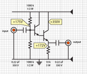
Well, as I said earlier, this is why the Darlington 2-transistor configuration is often deployed. For instance, the APT27ZTR 800 mW, 450 VCEO breakdown is 38¢ ea, and offers nominal hFE of 25 or so at 10 mA. Coupled to an APT13005SU, 60¢/ea … with heat sink able to handle 20 W, and with a 100 mA gain of 35, you get a mutual gain of 35 × 25 = 875 or higher.
Since the input impedance load is
ZIN = β ZLOAD where
β ≈ hFE ⊕ 1
for emitter-follower circuits, we can figure that a 25 kΩ load would deliver a 1 MΩ or higher input impedance. β ≈ hFE ⊕ 1
Not bad for a couple-of-bucks solution.
Just saying,
GoatGuy ✓
Last edited:
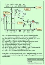
Update with ''more of the usual documentation''.
PS: this same diagram, substituting a lower voltage B+ power supply, can work quite well down to B+ = 20 volts or so. Of course, the dynamic range gets squeezed substantially. But on the upside, the maximum tension (voltage) of the capacitors also is similarly reduced. Making for less expensive, smaller and more compact caps. Also making for much lower voltage requirements for the power supply and for the Q1, Q2 transistors. Indeed, below about 150 V supply, easily obtainable Darlington-in-one-package transistors can be used.
GoatGuy
Attachments
Last edited:
The KSC5026M is a fake transistor aimed to be used as a switch. As an amplifier it will generate massive distortion.
Crss does not increase much but it is always there. The series Darlington coupling involves a huge capacitance coefficient, that is, very high current gain and a very modest bandwidth.
Capacitance is not an issue with Mosfets when used as source followers.
Crss does not increase much but it is always there. The series Darlington coupling involves a huge capacitance coefficient, that is, very high current gain and a very modest bandwidth.
N101N,
One nice thing about a MOSFET is you can drive the gate voltage all the way up to the Drain Voltage.
So you can use it for large voltage swings as a Source Follower.
But take care choosing a MOSFET. The poor old IRF150 has the following: Crss 450pF at 10V Drain to Gate, Crss 50pF at 50V Drain to Gate.
Tube Cathode followers are normally not that bad (not the capacitance, and not the non-linearity of capacitance). Most MOSFETs are much better than the IRF150. But you get the point.
As the source follows the gate you don't see the capacitance:
The input capacitance of a source follower configuration shown in Figure 1 is defined as the sum of the gate to drain capacitance, and gate to source capacitance multiplied by, 1 minus the gate to source gain, so:
Cin = CGD + CGS(1 - AGS)
Where: AGS = RS / RS + (1/gm) if the drain resistance is much greater then the source resistance as is often the case (rd >> RS).
I was looking at STP3NK60ZFP which has internal zener, and has an insulated tab.
Agreed the valve is better but may require a elevated heater source. I think it 200v but 150v max cathode - heater is safer.
baudouin0,
Yes, good formula. But those capacitance numbers change versus voltage. Look at the family of capacitance curves versus voltage. Plug in the numbers for one voltage, figure the total gate capacitance. Then plug in the numbers for another voltage, figure the total gate capacitance.
My main point was the changing capacitance. It can be a contributor to non-linearity.
- Status
- This old topic is closed. If you want to reopen this topic, contact a moderator using the "Report Post" button.
- Home
- Amplifiers
- Solid State
- Transistor cathode follower