Very simple bridged amplifier
I have decided to build a new class AB amplifier, that would be simple enough but would have parameters good enough and some power for a common home listening conditions with average speakers, 85 – 90 dB/W/m sensitive. I did not want to make a complicated SOTA design, and also wanted to utilize my nice power supply with a 300VA double secondaries toroidal transformer, which has quite a low output voltage. With this transformer I get 2 x 27Vdc supply voltage, with separated windings for left and right channel rectifiers and filters, which eliminates loop issues.
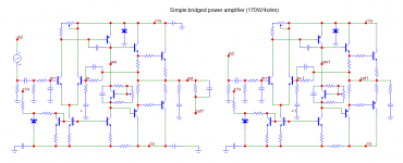
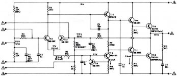
The amplifier circuit is based on a 50 years old Sinclair Z-30 topology, however considerably modified to better output devices (MJL21193/94) and with highly improved PSR by new input differential stage CCS design. The goal was to get more than 100W/4ohm, so the bridged concept was used as the only possibility with only 2 x 27V power supplies. Bridged amplifier has some special properties like cancellation of even harmonics distortion, cancellation of CMV supply ripple components and no pollution of signal common (ground) by speaker currents. It also has 4 times higher output power than the same single amplifier operated with the same power supply voltage. As of cons, output devices have to handle 2x higher output current and output impedance is 2x higher compared to a simple amplifier.
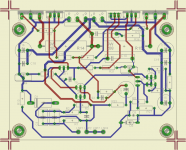
PCBs were designed and they are just in production to verify an amplifier prototype. Each board (80 x 100mm) makes a single simple one channel amplifier and 4 boards are to be used for a stereo, bridged amplifier. On the other hand, it is possible to build a simple, non-bridged version as well. A simple amplifier should give about 45W/4ohm, the bridged version is supposed to give about 170W/4ohm. Simulations are promising and the amplifier might have harmonic distortion of 0.002%/10W/4ohm and 0.02%/100W/4ohm at 1kHz. Only slight increase to 0.006%/10W/4ohm at 10kHz. The prototype is expected to be built in about 3 weeks.
I have decided to build a new class AB amplifier, that would be simple enough but would have parameters good enough and some power for a common home listening conditions with average speakers, 85 – 90 dB/W/m sensitive. I did not want to make a complicated SOTA design, and also wanted to utilize my nice power supply with a 300VA double secondaries toroidal transformer, which has quite a low output voltage. With this transformer I get 2 x 27Vdc supply voltage, with separated windings for left and right channel rectifiers and filters, which eliminates loop issues.
The amplifier circuit is based on a 50 years old Sinclair Z-30 topology, however considerably modified to better output devices (MJL21193/94) and with highly improved PSR by new input differential stage CCS design. The goal was to get more than 100W/4ohm, so the bridged concept was used as the only possibility with only 2 x 27V power supplies. Bridged amplifier has some special properties like cancellation of even harmonics distortion, cancellation of CMV supply ripple components and no pollution of signal common (ground) by speaker currents. It also has 4 times higher output power than the same single amplifier operated with the same power supply voltage. As of cons, output devices have to handle 2x higher output current and output impedance is 2x higher compared to a simple amplifier.
PCBs were designed and they are just in production to verify an amplifier prototype. Each board (80 x 100mm) makes a single simple one channel amplifier and 4 boards are to be used for a stereo, bridged amplifier. On the other hand, it is possible to build a simple, non-bridged version as well. A simple amplifier should give about 45W/4ohm, the bridged version is supposed to give about 170W/4ohm. Simulations are promising and the amplifier might have harmonic distortion of 0.002%/10W/4ohm and 0.02%/100W/4ohm at 1kHz. Only slight increase to 0.006%/10W/4ohm at 10kHz. The prototype is expected to be built in about 3 weeks.
Attachments
How are you going to connect it in a bridge configuration?
By the way I still have Z30 working version with 2N3055 OPS.
Z30-Z50 attached
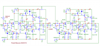
It is connected in a bridge exactly as shown in the image. Inputs are driven from preamplifier with a balanced output. In simulation, signal source is connected between the inputs, which is equivalent to a balanced drive.
I know original Z30-50 modules very well. I did like the topology with differential input and CCS loaded VAS, in the seventies. However it had issues. Quasi-complementary output stage, no emitter resistors in the output stage and thus very low idle current (high crossover distortion) to prevent a thermal runaway, no circuit to control thermal dependence of the idle current. Those zero emitter resistors were a headache, thermal runaway and second breakdown were so usual.
Last edited:
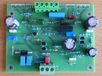
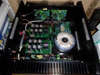
So, it looks like finished ") . The power supply gives only +/-25Vdc and +/-23Vdc under full load, so I get less power than expected, like 2 x 120W/4ohm. 4ohm is quite a heavy load, as each amp in the bridge "sees" 2ohm then. Output impedance is 0.026 ohm. Photos and schematics attached.
. The power supply gives only +/-25Vdc and +/-23Vdc under full load, so I get less power than expected, like 2 x 120W/4ohm. 4ohm is quite a heavy load, as each amp in the bridge "sees" 2ohm then. Output impedance is 0.026 ohm. Photos and schematics attached.
. The power supply gives only +/-25Vdc and +/-23Vdc under full load, so I get less power than expected, like 2 x 120W/4ohm. 4ohm is quite a heavy load, as each amp in the bridge "sees" 2ohm then. Output impedance is 0.026 ohm. Photos and schematics attached.Attachments
The simpler the circuit, the more benefits per balancing:
I would not use a "complementary-psu": + or - only
I would balance per transformer - never per output-signal (already strongly modulated;-)
Never use channel-separate psus - same idea/philosophy/experience like balancing;-)
I would not use a "complementary-psu": + or - only
I would balance per transformer - never per output-signal (already strongly modulated;-)
Never use channel-separate psus - same idea/philosophy/experience like balancing;-)
So, it looks like finished
Sometimes small value capacitors in parallel with a load can induce instability through some critical resonance at high frequency.
There are 10 pf lead capacitors in the nfb feedback arms of each amplifier plus zobel networks on the outputs of each amplifier connecting each output to ground.
C11 at 2nF is connected to each of these elements and at the same time the speaker is a reactive load which can generate out of phase signals.
At high frequency there is a low impedance path to the inverting inputs of each amplifier via the lead capacitors.
Since the nfb in each amplifier works in opposite phase the nfb of the partner will appear as pfb and there would be a double error correction which could promote IMD or instability.
Why didn't you use "blameless"-style single resistor between drivers' emmiters?
I am not sure that it has advantages only. I made some measurements telling me that both concepts have + and -.
Sometimes small value capacitors in parallel with a load can induce instability through some critical resonance at high frequency.
There are 10 pf lead capacitors in the nfb feedback arms of each amplifier plus zobel networks on the outputs of each amplifier connecting each output to ground.
C11 at 2nF is connected to each of these elements and at the same time the speaker is a reactive load which can generate out of phase signals.
At high frequency there is a low impedance path to the inverting inputs of each amplifier via the lead capacitors.
Since the nfb in each amplifier works in opposite phase the nfb of the partner will appear as pfb and there would be a double error correction which could promote IMD or instability.
C11 2nF is for simulation purposes only, same as R10 and there is a bold expression LOAD. I would have hoped this must been clear to anyone who can read schematics. Anyway I apologize this is a scheme from a simulator, some supply bypass capacitors not shown etc. The amplifier is tested for capacitive load from 0pF to 100nF without any stability issues. Cfb + Cdom + Zobel are tuned not only by simulation, but by measurements as well. Though I appreciate your comments, I would never let live an unstable amplifier.
Last edited:
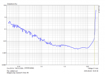
Some measurements in time domain:
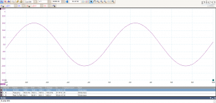
- 1kHz 93W/6.8ohm
- 100kHz 48Vpp/6.8ohm
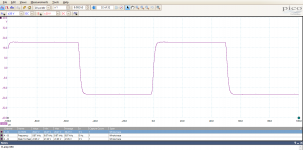
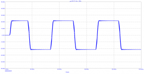
- 10kHz square 42Vpp/6.8ohm
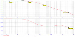
Good to see a 10kHz square wave included. I like to simulate with sample test capacitors in parallel with the load. In these I change the designation of the speaker load elements to CL or CTest rather than a component part number.
For the capacitor the value can be changed to {CV} and the command .step param CV list 5nF 10nF 100nF 220nF 470nF 1uF 2uF can then be used to check a personal choice selection of multiple values in one graph.
This test can show up the drive capacity needs attention - even when a Tian probe simulation shows the gain and phase margins to be more than satisfactory.
It appears that Miller capacitance is your dominant pole and the lead capacitor serves a trim purpose allowing a lower value Miller capacitor. The apparent aim is to maintain the slew rate of your voltage stages through matching the charging of this capacitor by available LTP current.
There should be no such issues with a lead capacitor being connected to the output which would seem to be a good idea and I can see why you chose this - a popular strategy for DIY designs if not with people like Self.
The lead capacitor feedback path is low impedance at hf and this will promote an increase in the rate of change and the signal phase which precedes reduction in gain by a decade in frequency.
How this works out in practice depends on a lot of things going right with establishing a dominant pole in real life conditions - loads, layout, etc.
An alternative approach can be seen in some versions of the Leach Low TIM amplifier ( which I built) and also used in Naim circuits.
In these a stopper resistor is inserted in series with the lead capacitor to create a step network. The decline in hf gain can then arranged to level out before a critical point is reached with change in phase.
In terms of stability margins I suggest this would be a safer option.
On the subject of bridge amplifiers you may be interested in some composite amplifiers based on AD711JN op.amps in combination with LM1875 modules.
The op.amp to improve the performance of the latter might be adaptable to a discrete component power amplifier such as your design.
In this the lead capacitor feeds the op.amp placed ahead of the power amplifier and the former unlike the latter would be stable at unity gain. The design includes all the inverting op.amps for bridge operation.
The link is ELECTRONICS NOW: Sucessor to Radio Electronics where you can select the issue from November 1992 and read from page 38 onward.
Scott Wurcer who is a member of our community is a co-author of the article.
For the capacitor the value can be changed to {CV} and the command .step param CV list 5nF 10nF 100nF 220nF 470nF 1uF 2uF can then be used to check a personal choice selection of multiple values in one graph.
This test can show up the drive capacity needs attention - even when a Tian probe simulation shows the gain and phase margins to be more than satisfactory.
Attached is the simulated result with CV list 5nF 10nF 100nF 220nF. Real measurements are in a good conformance, but sorry I am not going to repeat and save every measurement to bring an evidence.
Test with big capacitances >= 1uF is impractical, such situation will never happen with a standard electro-dynamic speaker. Such test also stresses output devices, even the rugged ones like those 21194/3 used. And it does not speak about amp stability, rather about L/C/R ratios.
In my experience, it is best to make conclusions on real circuits, real amplifiers and real measurements. Qualified predictions and guesses may be helpful, but also misleading, as something may be easily not taken into account. So I am very careful when making assumptions about circuits I have not built and tested. And then, every realization is unique.
Attachments
- Status
- This old topic is closed. If you want to reopen this topic, contact a moderator using the "Report Post" button.
- Home
- Amplifiers
- Solid State
- Very simple bridged amplifier 170W/4ohm