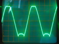
In you circuit, the drive into the base of Q7 continues after it has saturated. This causes the voltage drop across R12 to rise giving you the characteristic bump in the bottom half of the clipped waveform. Because the collector load of Q7 is a current source, you can be sure most of this excess current is being pumped into the base of Q7 via Q10.
During clipping, the amplifier is running open loop.
When the amp comes out of clipping, the loop tries to recover, and you get a large positive going spike - the mosfet input gate capacitance is also a contributor to this recovery problem.
To fix this issue, place a fast, small signal clamp diode with the anode on the base of Q10 and the cathode on the collector of Q7. you have a similar issue with Q8 at HF - i.e. 10 kHz.
I am not familiar with the VAS transistors you are using, but you should try to use fast, low Cob devices for best performance - I suspect Q7 is quite a slow device given the high recovery spike as it comes out of -ve clipping.
See here for more information Fast Voltage Amplifier Stages for Audio
Last edited:
And the VAS current will be large during this clipping, perhaps in excess of the device abs max value.
I'd strongly recommend a VAS current limiter transistor across R12 to draw base current away from Q7 or Q10 - calculate R12 so the current limit is somewhat over twice the standing current in the VAS output - distortion simulations can figure out if its causing any linearity issues at full swing - you can push the limit higher if so.
This may reduce VAS gain, but it also protects the VAS transistor from failure if the output locks up or the feedback loop gets broken somewhere. It prevents saturation and speeds up clipping recovery of course.
With the output locked up at the positive rail the VAS transistor will dissipate twice the rail voltage times the current limit, so check that its able to handle this (heat sinking may help), and the stage should be robust to cascade failure.
For instance 6mA VAS with a 15mA limit, with +/-45V rails would dissipate 1.35W in fault conditions, 0.27W normally and without the limit would immediate die on positive lock-up.
Try it at 100KHz, no load and see what it does?
In simulation, I do not think that it will characterize the clipping behavior as you would in real device operation. Do the scope and the sim wave forms match?
These are the reasons for a push-pull complementary type design.
In simulation, I do not think that it will characterize the clipping behavior as you would in real device operation. Do the scope and the sim wave forms match?
These are the reasons for a push-pull complementary type design.
Last edited:
If you add a clamp around the VAS as I suggested, you will not need to add any current limiting circuit to the VAS - see the presentation I linked to.
ctrlx - in the presentation are some circuits with the transistor types shown - try to sim with one of those. You need a fast, low Cob device.
ctrlx - in the presentation are some circuits with the transistor types shown - try to sim with one of those. You need a fast, low Cob device.
Clamping the VAS is pretty straightforward, and it is the first thing to be done, but eliminating saturation effects from the upper CCS is not so simple: ideally, you would want a schottky diode, but for higher voltages, it would be more difficult to find a suitable device.
It is possible, but it is probably simpler to use the original Baker scheme, with a diode in series with the base.
It is possible, but it is probably simpler to use the original Baker scheme, with a diode in series with the base.
Simple answer is a Baker clamp across the VAS. 1N4148 will do for starters, but a BAV21 is better. Anode from base of Q10, cathode to collector of Q7.
Also, why not add a driver stage for the MOSFETs rather than driving them directly from the VAS?
Same question by me - distortions drop significantly in simulation, specially at high frequencies. The only drawback I know is a slightly reduced max output level before clipping.
Clamping diodes on both the VAS (Q10+Q7)and Q8. Even 1n4148 has a limited voltage (75V, +/-37.5) but the Darlington two diode input means that you don't need a Schottky. You can add a diode in series with R16 to use a regular diode to clamp Q8.
My favorite way to current protect the VAS is a collector resistor for Q10 and then you can remove R12. Pick a resistor that limits the Q10 collector current to about 20x the Q7 base current and tap about 10x with R(can't read it ~R19 at the base of Q7). You may want to put a small (1nF) cap from Q10-C to V-.
This is different than an output where the output protection shifts the overload to the VAS, and then Mark's plan is the best. It may be required if the power FETs have internal gate clamping, which may not be modeled with standard spice models.
Note that spice models do not model break down (Vceo) voltages unless you make a macro that includes a zener.
Clamping diodes on both the VAS (Q10+Q7)and Q8. Even 1n4148 has a limited voltage (75V, +/-37.5) but the Darlington two diode input means that you don't need a Schottky. You can add a diode in series with R16 to use a regular diode to clamp Q8.
My favorite way to current protect the VAS is a collector resistor for Q10 and then you can remove R12. Pick a resistor that limits the Q10 collector current to about 20x the Q7 base current and tap about 10x with R(can't read it ~R19 at the base of Q7). You may want to put a small (1nF) cap from Q10-C to V-.
This is different than an output where the output protection shifts the overload to the VAS, and then Mark's plan is the best. It may be required if the power FETs have internal gate clamping, which may not be modeled with standard spice models.
Note that spice models do not model break down (Vceo) voltages unless you make a macro that includes a zener.
Dear Mark and steveu,
Please, ONE figure is worth a hundred words ! Please kindly post a small diagram to make your points ! Please ! Or a reference to a Pic ! Your posts are very useful. A pic will make them more useful to beginners !
--gannaji
Dear Mark and steveu,
Please, ONE figure is worth a hundred words ! Please kindly post a small diagram to make your points ! Please ! Or a reference to a Pic ! Your posts are very useful. A pic will make them more useful to beginners !
--gannaji
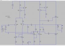
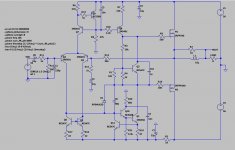
Agreed, but without the original asc file, we have to re-draw the whole thing.
Let me go find something similar and I will post it.
Meantime, clamping Q8 is rarely done. Popular is a base resistor for Q2 and for Q?9. These base resistors or a capacitor on Q?9 and Q2 are advised to guarantee stability of the current source.
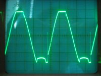
OK, this illustrates most of the points discussed here. I put a clamping diode in the circuit but it hardly does anything because the VAS can not be driven too far away from normal values anyway. Note that this simulation is deliberately driven to clip so THD is bad unless you reduce the input.
Attachments
Last edited:
I’ve got a topology that works reasonably well in my cascaded diamond amp - essentially clamp diodes on the VAS transistors, which are forward biased just prior to clipping using some transistors and zeners from the rail. It’s straightforward and works very well.
See https://www.diyaudio.com/forums/sol...eap-low-thd-10w-amp-tip41c-4.html#post5307265 for details.
I also found throwing diodes across other compensation caps helps things.
See https://www.diyaudio.com/forums/sol...eap-low-thd-10w-amp-tip41c-4.html#post5307265 for details.
I also found throwing diodes across other compensation caps helps things.
A resistor in the collector of Q10 works well to control peak VAS current. This is the technique dadod uses. In the pdf I linked to earlier you can see the performance of this approach and a simple voltage divider formula to calculate the peak VAS current you can expect.
Limiting the input current to the VAS is an alternative to the clamping diode to reduce rail sticking. If the normal VAS base current is 30uA then a 300uA limit does not affect normal operation but eliminates over-saturation. For a 50VDC rail that means the collector resistor needs to be 150K. The issue is complicated by a decoupling cap for stability but normally unnecessary.
- Status
- This old topic is closed. If you want to reopen this topic, contact a moderator using the "Report Post" button.
- Home
- Amplifiers
- Solid State
- improving clipping behaviour