Came across this website, where its maintainer appears everywhere but is almost impossible to contact
So a request to correct the last image please Ian.
FET Common Drain | Source Follower | Electronics Notes
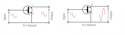
namely Drain and Source have inexplicably swapped in the last image.
So a request to correct the last image please Ian.
FET Common Drain | Source Follower | Electronics Notes
namely Drain and Source have inexplicably swapped in the last image.
For those who don't quite follow JFET operation, this interesting 2018 demonstration video covers just about everything there is to know about their strange properties - even their construction. The interchangeable Drain/Source topic begins about 6 mins in. It was amusing to see that On-Semi also state this symmetrical aspect clearly on their remaining JFET datasheets. YouTube
For those who don't quite follow JFET operation, this interesting 2018 demonstration video covers just about everything there is to know about their strange properties - even their construction. The interchangeable Drain/Source topic begins about 6 mins in. It was amusing to see that On-Semi also state this symmetrical aspect clearly on their remaining JFET datasheets. YouTube
Interchangeable should be clarified, to provide the three forms of connection
where one fet device is used, namely.
1. Common Source providing high input impedance and high gain
however potentially unstable.
2. Common Drain, providing high input and low output impedance
and if we include interchangeability to include the gate
3. Common Gate providing low input resistance and low input capacitance
Unconditionally stable but has lower power gain than common source
but has the best bandwidth of all three.
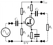
so briefly back to Ian Poole's diagrams Mooly is quite correct there is no description of resistance loading to the gate, or other features necessary for common drain connection
We see a very over simplified diagram then inexplicably change from Common Drain to Common Source, whilst offering the circuit description as a Common Drain .
Last edited:
Sorry but no: as shownIndeed: I think output C2 should be on drain not on source.
An externally hosted image should be here but it was not working when we last tested it.
the circuit is a properly working and properly labelled (on text body) source follower circuit, but image text wrongly calls it "common source" which it is not.
And first image is also very wrong, now on two counts:
An externally hosted image should be here but it was not working when we last tested it.
]1) no load resistors are shown, which is *very¨* confusing for those trying to learn how the circuit works and
2) signal is wrongly applied between Gate and Drain, while it should be applied between Gate and Source.
Of course poster shopuld reverse G and D pin labels.
As a side note, even if a FET is symmetrical, so "S and D are interchangeable" , once they are in a circuit "one of them must work as Source and the other one must work as Drain"
Even if they are "built the same and interchangeable" once in a circuit their function is different.
- Status
- This old topic is closed. If you want to reopen this topic, contact a moderator using the "Report Post" button.
- Home
- Amplifiers
- Solid State
- Dear Ian poole