AECA - Advanced error correction amplifier. Based on my work last months, it is my contribution to you tireless DIY-ers. Sims looks good, let you tell me if there is interest for PCB development. Of course, we can make it better together.
Attachments
Last edited:
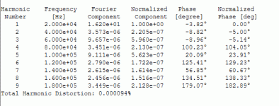
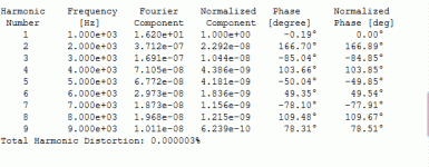
Few changes later, better sims and I think I will try it. Low level signals (2V) at 1kHZ shows zero. Looks stable on capacitive loads, at least looks same as some other amazing amps here. Layer is next step.
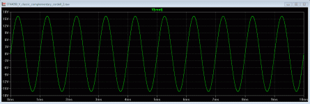
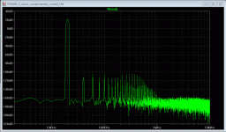
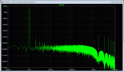
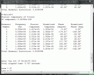
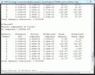
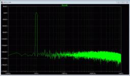
Pics: fft 1kHZ, amplitude 2V, THD 1kHz 2V, fft 1kHz 15V, THD 1kHZ 15V, fft, THD 20 kHZ, square 20 kHZ, rasponse.
Pics: fft 1kHZ, amplitude 2V, THD 1kHz 2V, fft 1kHz 15V, THD 1kHZ 15V, fft, THD 20 kHZ, square 20 kHZ, rasponse.
Attachments
-
 AECA_3.gif35 KB · Views: 106
 -
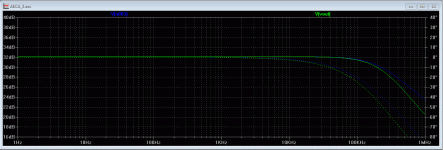 frequency_rasponse.gif22 KB · Views: 50
 -
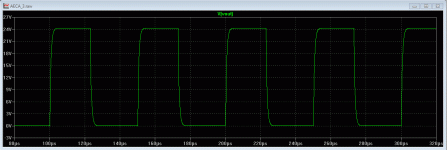 square_20.gif16 KB · Views: 55
 -
 THD_20_15v.gif25.4 KB · Views: 72
 -
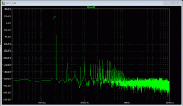 fft_20_15v.gif28.5 KB · Views: 67
 -
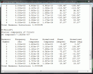 THD_1_15v.gif27.7 KB · Views: 66
 -
 fft_1_15v.gif26.9 KB · Views: 65
 -
 THD_1_2v.gif25.8 KB · Views: 68
 -
 fft_1_2v.gif25.2 KB · Views: 62
Looks interesting, but it is a little hard for me to see what's really going on. Care to give a little functional description / primer on theory of operation? I'd like to know a little more.
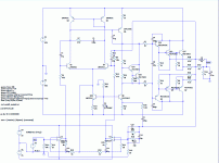
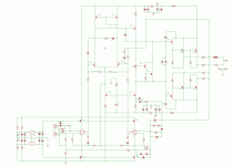
Sure. You will recognize classic amp schematic if remove opamps u1 and u2. Beauty is in there it is STK 40xx circuit basically and can be built with no settings. My prototype based on TDA 7294 works that way from first minute. But I noticed STK circuit suite that concept even more.
Idea is to increase gain from first stage by reducing emitter resistance of q1 and q3, what is achieved by u1 and u2 opamps. That two opamps close their loops on three stages, first one through c10, c11, compensating high frequency, second through q1, q2 emitters for linearization differential stage and increasing gain. Third is closed from output for amp control , negative feedback. Second one is most interesting, and for sure the one that is not easy to catch. On low frequency, that is audio band, the two are working by positive feedback through node between R18,R19 and collector q10. It keeps gain very high while frequency low, and keeps phase margin when signal from output start to late. It is because in that case positive feedback on stage two exceed to negative feedback what is achieved by proper adjusting first loop through c10, c11. It makes compensation possible even if gain on 20kHz is still high enough for good control over amp.
Please ask if you have further questions,
Best regards
A few very basic comments....
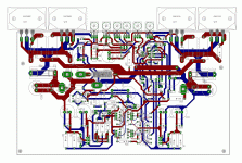
1) Is it a good idea to have the output inductor in the middle of the PCB? All those magnetic fields it can produce. Maybe better to be off board.
2) I may be blind but would it not be a good idea to have some local decoupling for the output transistors?
3) You could thicken some of the tracks. The copper is there to be used.
Please could you post the schematic that this PCB is designed from?
A few very basic comments....
1) Is it a good idea to have the output inductor in the middle of the PCB? All those magnetic fields it can produce. Maybe better to be off board.
2) I may be blind but would it not be a good idea to have some local decoupling for the output transistors?
3) You could thicken some of the tracks. The copper is there to be used.
Please could you post the schematic that this PCB is designed from?
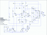
It is easy to remove inductor, if 10 turns air coil cause problems. Agree decoupling, will be added. Tracks are not finalized, your opinion works. Schematic follows.
Attachments
Thank you.
Looking at that you may need to consider minimum loading on the voltage regs. Also, local decoupling for the op amps would be a good idea.
I have come to the conclusion the most important part of a PCB layout is getting the power rails right.
Have you considered doing a cherry style layout? Like the one I did for my amp. This is where you run the power rails down the centre of the PCB then lay everything out either. It is very easy to keep loops small this way and everything just falls into place.
Thank you.
Looking at that you may need to consider minimum loading on the voltage regs. Also, local decoupling for the op amps would be a good idea.
I have come to the conclusion the most important part of a PCB layout is getting the power rails right.
Have you considered doing a cherry style layout? Like the one I did for my amp. This is where you run the power rails down the centre of the PCB then lay everything out either. It is very easy to keep loops small this way and everything just falls into place.
Voltage regs. are stabilized reference, op amps are loading transistors on rails. It is decoupled by ones in view of hfe. Interesting, capacitive decoupled op amps runs into problems. This circuit works in practice very well for few months.
Rest of the circuit should be solved. Power through center of the board is interesting, I will think about it.
- Status
- This old topic is closed. If you want to reopen this topic, contact a moderator using the "Report Post" button.
- Home
- Amplifiers
- Solid State
- AECA