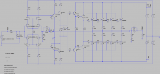
Somewhat high performance amplifier.
Complementary input with 2SK170/2SJ74 cascoded by 2SK246/2SJ103.
About 4 mA through each 2Sk170/2SJ74, 8 mA through R2.
Darlington VAS'es with 2SC3503/2SA1381. 9 mA though the VAS section.
Driver section with 10 mA through 2SC3503/2SA1381 pre-drivers and about 50 mA through MJE15032/MJE15033 drivers.
Output consists of 4 pairs of 2SK1058/2Sj162 Lateral FET's biased at 150 mA each.
Curerntly only done in simulation but the results are good enough for me to start building it soon, once I get the layout done.
Attachments
Last edited:
The tests below were done WITH the input filter and 470 uF cap in the NFB network.
THD-1 and THD-20 simulation results. 8 Ohm load.
THD-1
1 W : 0.0000375%
30 W : 0.000234%
60 W : 0.000391%
90 W : 0.000495%
THD-20
1 W : 0.000556%
30 W : 0.005390%
60 W : 0.006296%
90 W : 0.020645%
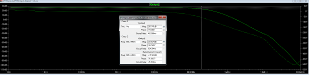
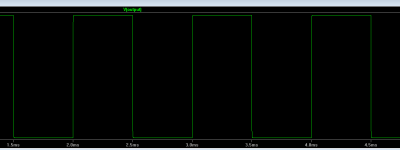
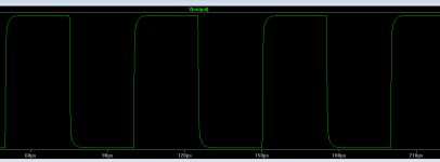
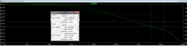
Attached images shows output frequency response and squarewave performance plots at 1 KHz and 20 KHz.
Gain is about 26.6 dB
Frequency response plot shows 26.2 dB at 1 Hz and a high frequency -3 dB point of 195 KHz.
THD-1 and THD-20 simulation results. 8 Ohm load.
THD-1
1 W : 0.0000375%
30 W : 0.000234%
60 W : 0.000391%
90 W : 0.000495%
THD-20
1 W : 0.000556%
30 W : 0.005390%
60 W : 0.006296%
90 W : 0.020645%
Attached images shows output frequency response and squarewave performance plots at 1 KHz and 20 KHz.
Gain is about 26.6 dB
Frequency response plot shows 26.2 dB at 1 Hz and a high frequency -3 dB point of 195 KHz.
Attachments
Last edited:
Below tests were done WITHOUT the input filter and the 470 uF cap in the NFB network.
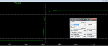
Attached are Loop gain and Slewrate measurement plots.
Loop gain plot shows about 69 degrees phase margin and about 10 dB gain margin.
Slewrate measurement plot shows a slewrate of about 60V/500nS, which scaled to 1us gives a slewrate of about 120 V/uS.
Attached are Loop gain and Slewrate measurement plots.
Loop gain plot shows about 69 degrees phase margin and about 10 dB gain margin.
Slewrate measurement plot shows a slewrate of about 60V/500nS, which scaled to 1us gives a slewrate of about 120 V/uS.
Attachments
Nice, but do you need the double emiter follower if you are using a FET output stage? You should be able to drop this to a simple emitter follower buffer between the VAS and the FET's.
Your loop gain plot looks a bit optimistic and in practice you may run into instability issues - I would shoot for a unity gain cross over frequency of around 1-2MHz. You can accomplish this by providing more degeneration on the JFETS, or increasing Cdom - but this latter appproach will cause your slrew rate to decrease unless you increase the LTP current.
The 10pF comp fap across your feedback resistor also looks a bit on the high side. This value should be set during development of the physical prototype, and it needs to be tweaked to give the optimum gain margin. For a feedback resistor values of 5k, this typically means about a 5-10pF capacitor.
You may want to consider using TMC instead of the miller comp currently shown in your designs - this will get your distortion down another 2x or more.
Good luck with your project.
Last edited:
Single EF driver stage is more than enough for lateral FETs, looks like BJT amp is adapted for laterals. 😀
Nice, but do you need the double emiter follower if you are using a FET output stage? You should be abel to drop this to a simple emitter follower buffer between the VAS and the FET's.
You may want to consider using TMC instead of the miller comp currently shown in your designs - this will get your distortion down another 2x or more.
Good luck with your project.
I tried with just a single emitter follower, THD-20 stayed at atleast 0.01% THD from 30 W and up. I think it was about 0.022% THD-20 at 60 W output. With the double emitter follower the THD-20 was alot lower to the tune of about 3x.
A single emitter follower loaded the VAS too much. Going from a single emitter follower to double emitter follower reduced the load on the VAS from 750uA to about 70-80uA. Which resulted in a nice reduction of THD-20.
Distortion wise I am more than happy at the current level, TMC really isnt needed.
Single EF driver stage is more than enough for lateral FETs, looks like BJT amp is adapted for laterals. 😀
Like I said in my reply to Bonsai, I started out with just a single emitter follower in the driver section. I didnt think it would be a problem. But my THD-20 simulations proved otherwise. Once I added the pre-drivers the THD-20 finally was where I expected it to be.
So it is NOT a BJT amplifier adapted to FET's. I started out with wanting to design a FET output amp.
Not my fault that it ended up looking like a BJT amp with FET outputs. 😉
Your loop gain plot looks a bit optimistic and in practice you may run into instability issues - I would shoot for a unity gain cross over frequency of around 1-2MHz. You can accomplish this by providing more degeneration on the JFETS, or increasing Cdom - but this latter appproach will cause your slrew rate to decrease unless you increase the LTP current.
The 10pF comp fap across your feedback resistor also looks a bit on the high side. This value should be set during development of the physical prototype, and it needs to be tweaked to give the optimum gain margin. For a feedback resistor values of 5k, this typically means about a 5-10pF capacitor.
Good points.
I'll take them into consideration.
Last edited:
Just out of curiosity; have you tried or considered a FET driver stage instead of the 3EF?
You are running the drivers very hot I see, personaly I would have there about 20 tot 30mA. Have you seen an improvement somewhere with increasing the bias throught the drivers?
Greetz
You are running the drivers very hot I see, personaly I would have there about 20 tot 30mA. Have you seen an improvement somewhere with increasing the bias throught the drivers?
Greetz
Just out of curiosity; have you tried or considered a FET driver stage instead of the 3EF?
You are running the drivers very hot I see, personaly I would have there about 20 tot 30mA. Have you seen an improvement somewhere with increasing the bias throught the drivers?
Greetz
I have considered a FET driver stage and am still considering it.
Driver current is something that could be adjusted. 20 mA would be just as reasonable.
I will be trying a FET driver stage tonight or sometime tomorrow.
If it comes close in performance I might go that way.
My goal is less than 0.01% THD-20 at 60 W into an 8 Ohm load as a minimum.
Last edited:
I have considered a FET driver stage and am still considering it.
Driver current is something that could be adjusted. 20 mA would be just as reasonable.
I will be trying a FET driver stage tonight or sometime tomorrow.
If it comes close in performance I might go that way.
My goal is less than 0.01% THD-20 at 60 W into an 8 Ohm load as a minimum.
Well, tried that, with irf510/9510 and irf610/9610.
Didnt work, 0.01% THD-20 for the 510/9510 pair and 0.02% for the 610/9610 pair.
The load on the VAS was still only 70-80 uA so that wasnt the problem.
I ran them with about 50 mA through them. Maybe they like a somewhat higher bias.
EDIT : 200 mA through 610/9610, same 0.02% THD-20. Looks like FET drivers in this amp is a dead end.
Last edited:
Recheck your output stage bias current if you ever adjust R3 or R27 in your sims. Because you are runnung at a high driver current, the base currents flowing throught your base stoppers on the EF transistors cause enough of a voltage drop to cause shifts in the bias point on the output devices. I would agree with the poster above, on a FET output stage, the drivers don't need to run at more than 20-30mA and still remain in class A
I always check the bias points, whenever I change R3 or r27 or adjust the bias.
Bias for the output stage is always set at 150 mA per FET.
Bias for the output stage is always set at 150 mA per FET.
just a tip - might be worth it to go to the hafler site, download the manual for the XL-280 and review the schematic.
mlloyd1
mlloyd1
I went back and did some more simulations with just one set of drivers. Out went the MJE15032/MJE15033 and now I'm only using 2SC3503/2SA1381 as drivers.
With 9 mA through them and still 150 mA per FET THD-20 is now 0.0068XX% at 60 W into 8 Ohm. Not quite as good as with the pre-driver/driver combo that got 0.0062XX% at 60 W into 8 Ohm, but taking into account that this is just simulation it could be considered just as good.
Slewrate is the same, both 1KHz and 20KHz squareware response look just as good.
Only downside is a reduction in phase margin but the gain margin shows an increase. Going from 61 to 50 degrees phase margin and from 10 dB to 18 dB gain margin.
But still, with this being just a simulation, performance is more or less the same, but with one less driver stage.
Took me all of 5 minutes to throw one driver stage out and retain more or less the same performance. 🙂
Only downside is a reduction in phase margin but the gain margin shows an increase. Going from 61 to 50 degrees phase margin and from 10 dB to 18 dB gain margin.
Apparently I cant read a Loop gain plot correctly.
What I ment to say was that phase margin stays at around 70 degrees and gain margin is improved to about 12 dB.
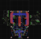
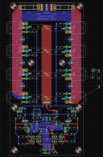
Preliminary layout, a work in progress.
From input to driver stage is more or less done. But wont rule any smaller tweaks to the layout before I'm done
It is not perfect but just as in more or less all layouts, some compromises have to be made.
From input to driver stage is more or less done. But wont rule any smaller tweaks to the layout before I'm done
It is not perfect but just as in more or less all layouts, some compromises have to be made.
Attachments
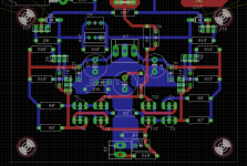
Layout almost done.
Considering some changes to the cascode, from JFET to BJT.
Alot easier to go with a BJT cascode.
However, simulations shows that the higher Vds voltage across the input 2Sk170/2SJ74 JFET, the lower THD-20 I get.
Somewhere around 20 Vds across the input JFETs give me the optimum THD-20 values. That is very close to the max Vds of the 2SJ74 JFET.
Difference from 20 Vds and something like 15 Vds is only an increase in THD-20 of 0.0015%. Not alot.
Attachments
assuming a fixed maximum voltage swing at the input fets, then with a high Vds that fixed input/output swing is a large portion of the total applied voltage.
Double or triple the applied voltage and the input/output swing becomes a much smaller part of the applied voltage.
That is what reduces distortion. The same logic applies to a VAS stage.
Double or triple the applied voltage and the input/output swing becomes a much smaller part of the applied voltage.
That is what reduces distortion. The same logic applies to a VAS stage.
- Status
- Not open for further replies.
- Home
- Amplifiers
- Solid State
- Complementary JFET-JFET cascode input, BJT VAS-Drivers, Lateral Output