I was just getting started with KiCad and looked at 15 videos and
There is great amp in here somewhere...
Any KiCad experts here? I would like a footprint of the BIG DIYAudio heatsink for KiCad and the like.
🙁🙁🙁
Thanks
I have an Idea that I will start a new thread on a little later. Bye and Thanks
There is great amp in here somewhere...
Any KiCad experts here? I would like a footprint of the BIG DIYAudio heatsink for KiCad and the like.
🙁🙁🙁
Thanks
I have an Idea that I will start a new thread on a little later. Bye and Thanks
@Krisfr,
I joined the thread too late to answer your previous questions about KiCAD usage. Since I use it extensively, let me know what help do you still need, I'll try to do my best.
I joined the thread too late to answer your previous questions about KiCAD usage. Since I use it extensively, let me know what help do you still need, I'll try to do my best.
2 questions, how do you handle 2 transistors in 1 package, as an IC? Do you have a diagram showing the individual computer files associated with each device component? In the line of which computer file is associated with the schematic representation of a transistor in a circuit, which file represents the 3d display, etc. etc.@Krisfr,
I joined the thread too late to answer your previous questions about KiCAD usage. Since I use it extensively, let me know what help do you still need, I'll try to do my best.
Attacks of any sort are not allowed on the forum. Some individuals will ad nauseamly pick and nit pick particular design typologies, but it is tolerated by some and hated by others. I asked for some help or thoughts and was deflected, so catch as catch can. I hope that in the vast group of Extremely knowledgeable people here, that a little bit more friendliness would be and automatically will be shown. If you don't agree with something, move on and go start your own thread. At least that is my thought. But if you can help, please do it and don't say "I know how" but I want you to show me if YOU can.
Thanks
I suspect there are several ways to tell KiCad about a single package which contains two transistors. Here is the way that I would do it, myself, on a Toshiba 2SK2145 dual transistor (see attached image).
I would treat the 2SK2145 as a semiconductor device which happens to have 5 pins, whose names are G1, D1, G2, D2, and S. This is the same general idea that's already used by several other devices:
I would create a schematic symbol for the 2SK2145 which has 5 pins, and whose graphical drawing shows two NJFETs with common source.
I would create a PCB layout "footprint" for the 5 pin package in which the 2SK2145 is supplied, and store it in my footprint library. Done.
There may be other ways to do it in KiCad. There may be better ways to do it. But this is the way I would do it. Or at least it is the first idea I would try.
_
I would treat the 2SK2145 as a semiconductor device which happens to have 5 pins, whose names are G1, D1, G2, D2, and S. This is the same general idea that's already used by several other devices:
- The 1N4148 is a semiconductor device which happens to have 2 pins, whose names are Anode and Cathode.
- The 2N3904 is a semiconductor device which happens to have 3 pins, named C, B, E.
- The IRFD224 is a semiconductor device which happens to have 4 pins, named G, D, S, D.
I would create a schematic symbol for the 2SK2145 which has 5 pins, and whose graphical drawing shows two NJFETs with common source.
I would create a PCB layout "footprint" for the 5 pin package in which the 2SK2145 is supplied, and store it in my footprint library. Done.
There may be other ways to do it in KiCad. There may be better ways to do it. But this is the way I would do it. Or at least it is the first idea I would try.
_
Attachments


Last edited:
Thanks a lot. Very well explained. I don't know any other place where this has been explained in a single page this neatly.
Krisfr, there are tutorial videos from Digikey and others on YouTube which explain how parts and symbols for new devices are added to the KiCAD libraries., The multi-part symbols are a bit more complex to set up and use, though not difficult. I learned the stuff from the videos.
Krisfr, there are tutorial videos from Digikey and others on YouTube which explain how parts and symbols for new devices are added to the KiCAD libraries., The multi-part symbols are a bit more complex to set up and use, though not difficult. I learned the stuff from the videos.
Yes thanks for your assistance. I found this page and it is very helpful. File Formats | KiCad EDA
and this...[solved] Import component in multiple unit component - Schematic - KiCad.info Forums
and this ...YouTube
I will post the solution to this as soon as I have a full schematic part, foot print and 3d symbol made for it and for the TO-264. So much to learn and trying to do the final work on it too.
Last edited:
Krisfr, I don't know if this can help ?:2 questions,
https://www.diodes.com/assets/Package-Files/SOT26-Type-CJ.pdf
https://www.diodes.com/assets/Package-Files/SOT26-SC74R.pdf
Last edited:
@Krisfr,
I was going to direct you to the KiCAD forum but I saw you've already found it 🙂.
There are a few things you must realise when working with KiCAD:
- In order to ease your life its highly recommended to organise your files (electric components, footprints, 3D-models) into well-known folders (known to the KiCAD SW via PATH environment variables). I'm attaching here the PATH variables in my KiCAD. I use Linix so the absolute paths may differ. The most important thing, however is the addition of my own PATH variables to the standard ones (KIMYLIB, KIMYMOD, KIMY3DMOD). They represent the paths to the folders I store my own symbols, modules (a.k.a footprints) and 3D models.
- Unlike some other EDA packages KiCAD uses a concept "one-to-many" which means you're not required to have relation "one electrical symbol - one component". On the contrary - you can use only one electrical symbol for NPN transistor and subsequently to assign to all transistors in your schematic particular footprints. This is done using so-called CV-PCB program module. So, it's not necessary to have a numbers of electrical symbols named for example BC550, BC547, BC546 etc. You can use only one NPN electrical symbol and assign different footprints to any of them.
For your question about dual transistor unit - in EeSchema firstly check the section "Devices" - I hope you'll find an electrical symbol which will best suite your needs. Then, if there's no suitable one, you can use an existing one as a "basis" for creating your own symbol.
Well, I can write a lot more but I think there's not the right place - if someone opens a tread about KiCAD I'll be glad to share my humble experience 🙂 there.
Attachments
Last edited:
Well I have done a lot of YouTube viewing and playing with KiCad and Fusion 360. Whew.
So now I have decided to make three 3 things.
1. The dual transistor SMD device.
2. The TO-264 or similar transistor case, that can be used for BJT or FET.
3. A resistor. Well at least a very special resistor.
I will be using the parametric systems inside of Fusion 360 and applying the generated files to KiCad.
Also I will do the layout in KiCad using some rounded corners and a few other nice looking techniques to do it.
Please feel free to add suggestions and comments. I also will be establishing a GitHub account for downloading the above and maybe some other things.
Thanks
I'm suggesting you to look at the existing libraries and modules which came with the installation of KiCAD. If you think there's a module which you want to use but with some "tweaking", you can copy this module to your own folder and modify it at your taste.
BTW, on Linux the standard libraries are installed in folders with read-only access from regular users so even if you want to modify some module, you won't be able to do this. That's why the only way to modify it is copying in some of your defined folders and edit it after.
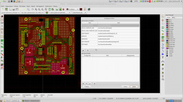
As you can see on the pictures below I split the footprints to several folders - Diodes, Resistors etc.
When copying the module I chose the appropriate folder to copy in.
BTW, on Linux the standard libraries are installed in folders with read-only access from regular users so even if you want to modify some module, you won't be able to do this. That's why the only way to modify it is copying in some of your defined folders and edit it after.
As you can see on the pictures below I split the footprints to several folders - Diodes, Resistors etc.
When copying the module I chose the appropriate folder to copy in.
Attachments
Interesting discussion about Soldermask minimum width:
Solder Mask Too Large in Gerbers and OSHPark but Screen OK - Layout - KiCad.info Forums
and a similar FAQ: "How does solder mask layer work?":
How does solder mask layer work? - FAQ - KiCad.info Forums
Written for KiCAD users but I suppose the principles are the same for the other EDA packages too.
Solder Mask Too Large in Gerbers and OSHPark but Screen OK - Layout - KiCad.info Forums
and a similar FAQ: "How does solder mask layer work?":
How does solder mask layer work? - FAQ - KiCad.info Forums
Written for KiCAD users but I suppose the principles are the same for the other EDA packages too.
I am having a great deal of trouble understanding the Library system of KiCad. Does anyone know of a picture diagram of the entire system, with a indication of which Sub-directory the library is located in? If one does not exist I want to make one. Any suggestion as to really understanding this phase of the system? I am working with it, but it is hard. Thanks
Hello
I nearly always create my own symbols and attach them to the footprints (and also mod the prints as well).
I use the bleeding edge nightly versions...
I have created my own symbols for dual transistors lately in where I place a transistor symbol, then right click to "edit with symbol editor", then I duplicate the symbol (on left side), then click the duplicated symbol (on left), rename it, then I get to work selecting the symbol and duplicating it, rotate it, mirror if needed, placing things here or there, rename and number the pins if necessary, and save it..
I'm a pro at dealing with it
if you need a demo video, lemme know, i'll whip one up 4u
ThanksSee if this helps..
You'll need to intuit some things here, just a mock up, but this is the gist of how I do it
YouTube
I am having a great deal of trouble understanding the Library system of KiCad. Does anyone know of a picture diagram of the entire system, with a indication of which Sub-directory the library is located in? If one does not exist I want to make one. Any suggestion as to really understanding this phase of the system? I am working with it, but it is hard. Thanks
I thought I've managed to explain this but I'll try this again:
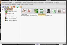
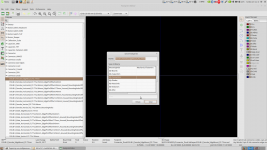
1. Open EESchema. Go to "Preferences" -> "Configure Paths"
There you can see the "EnvironmentVariables" which means the path to the library folders and its Variable Name

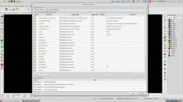
2. Close the window with Paths and open "Preferences" -> "Manage Symbol Libraries"

Here you cane see The NickName of the Library, the full path to the library file(s), type of the Library and description (if any). The string in the curly braces is actually the "Variable Name" defined in the window, shown on the first picture. So, actually ${KICAD_SYMBOL_DIR}/4xxx.lib translates to /usr/share/kicad/library/4xxx.lib on my system. If you use Windows, you'll definitely have a different first part, but the remaining must be the same.
As you can see the symbol library is a file which contains multiple electrical symbols grouped by given pattern.
3. The same is situation with the footprint libraries:

The library files names end with ".pretty" and any library file contains multiple footprints grouped by some pattern.
4. 3-D files reside in the folder defined with the PATH Variable "KISYS3DMOD".

Inside the folder are placed multiple folders which actually contain the 3-D files:

KiCAD supports VRML and STEP 3-D file formats and in the folders exist both types of files for any entry:

That's it for now, hope I was useful.
Hello
I nearly always create my own symbols and attach them to the footprints (and also mod the prints as well).
I use the bleeding edge nightly versions...
I have created my own symbols for dual transistors lately in where I place a transistor symbol, then right click to "edit with symbol editor", then I duplicate the symbol (on left side), then click the duplicated symbol (on left), rename it, then I get to work selecting the symbol and duplicating it, rotate it, mirror if needed, placing things here or there, rename and number the pins if necessary, and save it..
I'm a pro at dealing with it
if you need a demo video, lemme know, i'll whip one up 4u
The nightlies also have copy/paste, which might ease this workflow a bit.
Cheers,
Jeff.
@Krisfr, if you still have questions on the library system, fire away.
One thing to note: the variables are used because the actual storage locations are platform-specific. So let us know what platform you're using too.
Cheers,
Jeff.
One thing to note: the variables are used because the actual storage locations are platform-specific. So let us know what platform you're using too.
Cheers,
Jeff.
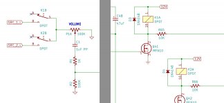
Symbol units are also a good solution for multiple transistors in a single package. They allow you to insert each transistor separately into the schematic, so that the layout doesn't always have to be identical. For instance:
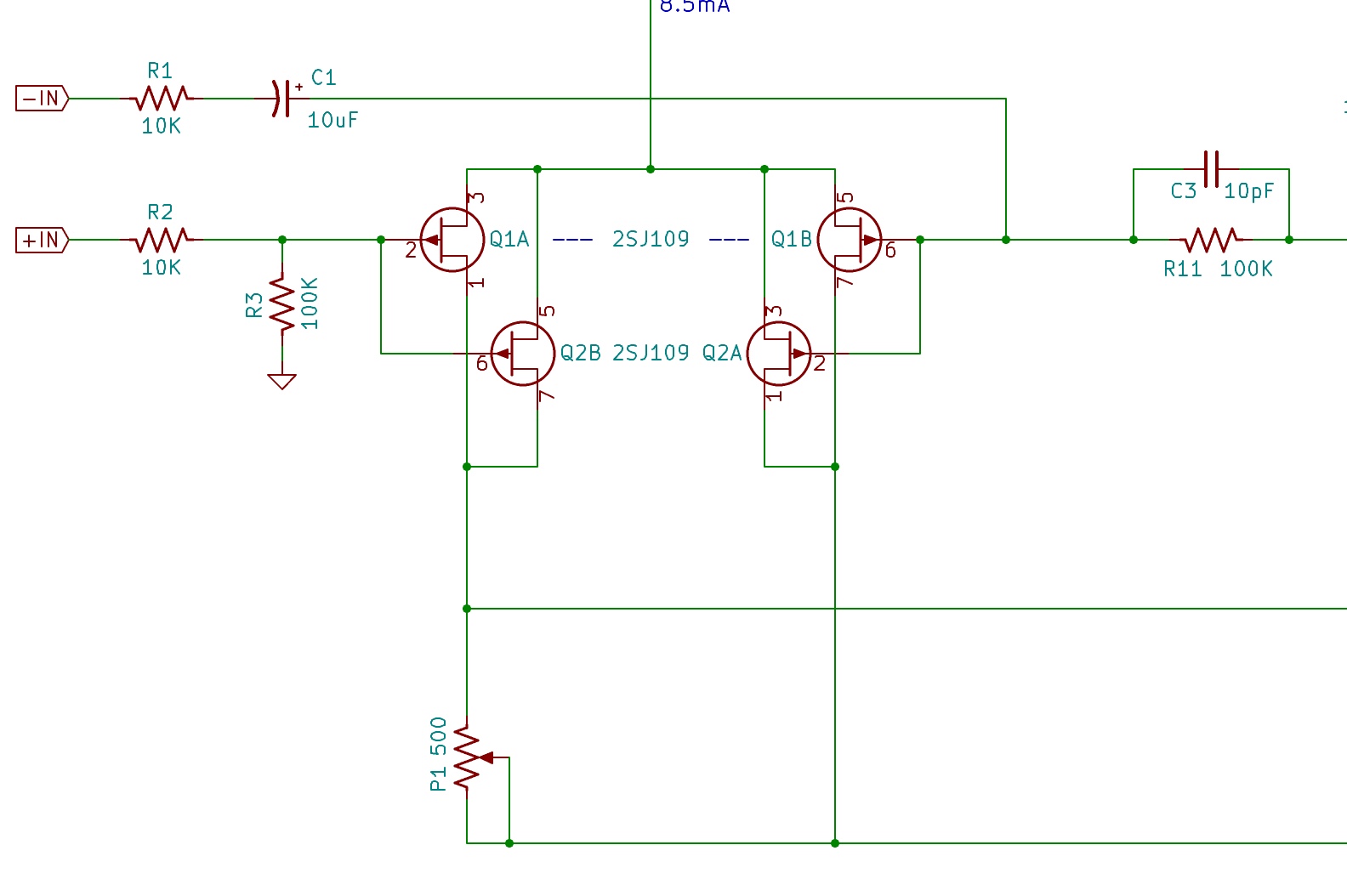
Same for something like a relay, where you want the coil on one part of your schematic and the switch on another:
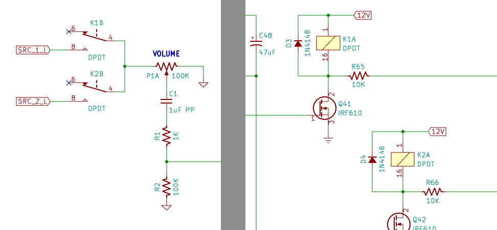
Same for something like a relay, where you want the coil on one part of your schematic and the switch on another:
Attachments
- Home
- Design & Build
- Software Tools
- KiCad Fusion360 Python for PCBs