Top layer: pcbname.GTL (K1 - Copper top)
Bottom layer: pcbname.GBL (K2 - Copper bottom, NOT mirrored)
Solder Stop Mask top: pcbname.GTS (Soldermask top)
Solder Stop Mask Bottom: pcbname.GBS (Soldermask bottom)
Silk Top: pcbname.GTO (B1 - Silkscreen top)
Silk Bottom: pcbname.GBO (B2 - Silkscreen bottom)
NC Drill: pcbname.TXT (Drill data)
Then you simply can rename the files.
The GTL and GBL etc extensions they ask for are just their naming convention, so you just need to rename the Gerber file output from Sprint-Layout to match their requirements.
Email them if you are not sure which drill options in Sprint-Layout to use. I usually use 3.2 metric, but that's with other PCB fabs.
Email them if you are not sure which drill options in Sprint-Layout to use. I usually use 3.2 metric, but that's with other PCB fabs.
The GTL and GBL etc extensions they ask for are just their naming convention, so you just need to rename the Gerber file output from Sprint-Layout to match their requirements.
Email them if you are not sure which drill options in Sprint-Layout to use. I usually use 3.2 metric, but that's with other PCB fabs.
Thank you!
I see. These drill options have to do with standard holes that they will have to drill? I mean, the holes I will specify in my files should be a standard size chozen over a certain known range? Is this what this means?
It's not that, it's the format the NC drill info is written in, the way the XY coordinates are written in the file.
PCB fabs will have a range of drills so there shouldn't be a problem. The only thing that might come up is specifying metric drill sizes and sending the Gerber to a fab house in the USA where often imperial sizes are more common. That said, even they are starting to use metric a lot nowadays.
PCB fabs will have a range of drills so there shouldn't be a problem. The only thing that might come up is specifying metric drill sizes and sending the Gerber to a fab house in the USA where often imperial sizes are more common. That said, even they are starting to use metric a lot nowadays.
So I would like to order some pcb's from seeed, and I am a bit confused about how I should order a single copper layer pcb.
My options are:
Solder side (bottom) consists of : copper layer, soldermask + silkscreen, and:
(1) Component side (top) has only silkscreen.
(2) Component side (top) has through hole pads that come from the solder side (but no copper tracks), soldermask + silkscreen.
So, how do I implement the 2 options? Seeed asks for every layer (so how could I specify that I need no soldermask and copper, for case 1?). For option 2, I assume I just have to choose the option saying "through pad" for pads. Correct?
Look for Excellon format output, that is the standard drill format, use same settings as for Gerber.
You would be better using 3.4 metric format for both, better quality output especially if any circular interpolation is going on.
What is the difference between single and double sided boards from seeed?.
Single sided PCB:
Copper bottom,
Resist Bottom,
Component Ident Top,
Drill data Excellon,
If you are going for PTH holes then you'll require a copper top with the annular rings for the pads, of course you will have to pay for the plating process.
Richie00boy, when selecting the "add pad" option, I have access to a "Through pad", which corresponds to F12. Maybe I have a different version than you. 
Marce, yes Sprint Layout has Excellon format drill information. Seeed wants it in text, so my job is to export it to Excellon, and then rename it to .txt, right?
Also, do you suggest that to create a single sided board in seeed, I choose "1 layer" and add just these 4 gerber files you mention? Have you done it before?
Of course, I was thinking about going PTH since seeed seems to have the same price for both 1 or 2 layer boards. So, why not if it is trivial designing it?
Excellon is a n ascii (raw text) format, check it is what is called extended excellon (or excellon 2) this is the newer format and has the drill size information in the header.
There are a number of extensions used, .spl .drl etc. They should recognise the format when they read it into there front end system.
It would be a good idea to get a gerber viewer and look at yours outputs to check they are right.
GCPrevue is one option.
GraphiCode - Software Innovations for Electronics Manufacturing - Gc prevue
Also it is a good idea to include a readme.txt in with the gerbers that specifies which gerber is which layer in the stack, overall board dimensions, copper thickness, layer stack, minimum track and gap, standard or high Tg material, basically all the things the board house might have questions about.
Granted that this becomes more critical as number of layers increases and as you get into such esoterica as stacked microvias and selectively plating edge connectors, but I would consider it best practise anyway.
Something like this (for a 2 layer, 70um copper, high temperature board (RF Power amp)):
Project name : HF PA
PCB Version : 1.0
Dimensions : 100 x 160mm
Gerbers and drill file are : Metric 3.4
Number of layers : 2
Copper thickness : 70um
Minimum T/G : 0.2mm.
Minimum anular ring : 0.15mm
Board material : Tg150
Plating: ENIG
Drill file :HF_PA.exc
Top silk : HF_PA.GTS
Top resist : HF_PA.GTR
Top Copper : HF_PA.GTL
Bottom Copper : HF_PA.GBL
Bottom resist : HF_PA.GBR
Bottom silk : HF_PA.GBS
Just to give you an example of the sort of thing that should go with the gerbers, I am sure Marce will have more on this.
73 Dan.
Thank you all for the nice responses.
Marce, I will certainly have a look at my stuff with the aid of a Gerber viewer.
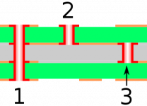
Richie00boy, this is what I meant, sorry if I confused you. And this positioning of pad both on top and bottom comes along with that rigid vias we talked about before, right? As it can be seen in the following picture - case 1:

Dmills, thanks for the tip.
Marce, I will certainly have a look at my stuff with the aid of a Gerber viewer.
Richie00boy, this is what I meant, sorry if I confused you. And this positioning of pad both on top and bottom comes along with that rigid vias we talked about before, right? As it can be seen in the following picture - case 1:

Dmills, thanks for the tip.
PTH is not specified by software usually. There may be some high end packages that allow selective plating. Usually you just tell the board house if you want it or not, and they do all or none. When having double sided PCB, PTH is usually done by the board house as a matter of course.
Last edited:
- Status
- This old topic is closed. If you want to reopen this topic, contact a moderator using the "Report Post" button.
- Home
- Design & Build
- Software Tools
- Spint Layout into Gerber