Hello to All:
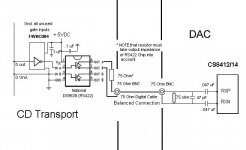
I have attached a schematic of an SPDIF circuit that
bridges between an RS422 transmitter chip and a
Crystal CS8412 reciever chip using a 75 ohm line
and 75 ohm BNC connectors.
Does anyone have opinions as to how well this
circuit would work between a transport and a DAC?
Any appraisals and/or revision suggestions would
be greatly appreciated!
Thanks!
Fastcat
Attachments
You asked.......
YUK!
That 47 pF cap has to go.........
I have made numerous posts stating that you should not connect the Crystal RX directly to the line.
Differential drive should be ok........I have no idea how well balanced the outputs are. Most try to stick an inverter in the circuit to create balanced. Too bad no one ever catches on to the additonal propogation delay on one leg.
Jocko
Jocko:
What is wrong with having the 47pF capacitor in
parallel with the DAC SPDIF input?
If the CS8412 should not be directly connected
to the input, through what should the incoming
signal go through (other than an excellent digital
pulse xformer)?
It seems that you are saying that there might be
a propigation delay using the 2 outputs shown
in my schematic with the RS422 chip ("out" and
"out-not", so to speak). Would it be better to use
only the RS422 chip "out", and take the shield lead
of the digital cable to GND inside the transport PS
circuit?
Also, is there any consequence by having an in-
verter gate before the RS422 chip on the 'xport
side of the circuit?
Many thanks for any input!
Fastcat
47 pF: The input impedance now has a strong reactive component. It has to be resistive.
Most digital pulse transfomers are poor. I use them, but I know some tricks to swamp out the leakage inductance. This value has to be as low as possible, which implies tight coupling. The opposite of what the "experts" think.
Stick some sort of linear stage in front of it. Be aware that any circuit will slightly affect the input Z.
The way to make a balanced output is to use XOR gates. You can get opposed phases without extra prop delay that most of the circuits on the 'net have.
That chip may do it the right way, as us "analog" guys" would use some sort of differential stage. They probably don't give details on the guts of it. But........it will be easy to check on a dual trace 'scope.
I would stick with the balanced version, but be aware that your shield is now "hot", and EMI may go up some.
As for the inverter.....if it is in a hex package, and the other ones on working, the jitter will go up.
Jocko
Jocko:
The ideas about the 47pF cap make sense.
I have read that the quality of the loading
resistors used in the SPDIF circuit (75 ohm)
can make an audable difference, and I will be
using Caddock units.
As to the inverter chip in my schematic, I was
planning to ground the inputs of the unused
gates, but is the inverter gate really necessary
between the digital signal and the RS422 chip?
Or can I go direct to the RS422 chip input?
Thanks again!
Fastcat
Save your money..........you could hook up $6 resistors with leads that are too long (i.e. inductive), and will sound like crud.
If your circuit puts out the right logic level, then why run it through another jitter prone part? I think a lot of time guys use that extra inverter just to use it. And add jitter in the process.
Reclocking is one thing that you might think of, if you have a clean clock source. Which you should have in the first place.
Jocko
- Status
- This old topic is closed. If you want to reopen this topic, contact a moderator using the "Report Post" button.