 This thread has been merged with posts from here - D-Noizator: a magic active noise canceller to retrofit & upgrade any 317-based V.Reg.
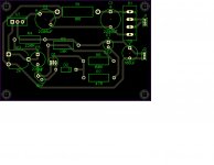
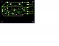
 Hi guys, I would be grateful if someone might cast an experienced eye on this PCB layout I have come up with for a single rail LM317 denoiser board. 🙂
It's sized to replace the old PSU board of a preamp I have built, it will be interesting to compare this to the old LM317
***
Hi all, I am trying to put together a PCB for a single polarity LM317 Denoiser and with the help of a few other members I have gotten this far.
The point of the exercise is to be single sided so that it can be etched at home if desired, there are many excellent fab PCB designs available but I haven't found a simple single sided one.
Still to do is to align the resistors vertically if possible, change the type of potentiometer and to make a single PCB but dual mono layout.
Attachments
Last edited by a moderator:
TO220 always to the side for mounting on casing or external heatsink. Even with a clip on heatsink heat is better kept away as far as possible
Larger footprint for C1 and C2 (or use 2 footprints) and please align them
Larger footprint for C7 (or use both)
Align C5, C7 and C8
Align R4 and R5
Revise GND PCB track!
it would be OK to have a bit wider PCB tracks especially where power flows
Use a film cap close to the input pin of LM317
Larger connector for J1 and J2 i.e. Phoenix MKDSN (or use both footprints)
Choose standard footprint for R2 as that format is pretty obsolete by now (or have both footprints)
Use smaller footprints for resistors that don't dissipate power
Put the 10 nF horizontal and a bit to the right
Q1 to the right and D2 a bit lower
You could put D2 vertical and R6 and R7 too maybe it creates space
I think all resistors can be aligned (and mounted vertical) except for R1
Last edited:
Is this for small current application? If it is not a limit imposed by design software, I would use much thicker PCB traces for ground and current carrying lanes. Rectifier could be rotated by 180 deg. and ground will go all around core circuit, so some copper pouring (zones) can be used.
I use ADM7150 and ADP7118 regulators in my DAC. They have proven to be excellent just around digital signal processing due to their characteristics, especially the ADM7150 which is an RF regulator. They are available in a SOIC8 case which is OK for DIY.
When I started making DACs about 15 years ago, I also used the LM317, but I quickly replaced it with better shunt type regulators.
And a very important note; a regulator that is good for analog signals in most cases will not be good with digital signals. For digital signals the frequencies in the MHz band are essential and the regulator must be ready to deal with them, the LM317 certainly does not belong there.
TO220 always to the side for mounting on casing or external heatsink. Even with a clip on heatsink heat is better kept away as far as possible
Larger footprint for C1 and C2 (or use 2 footprints) and please align them
Larger footprint for C7 (or use both)
Align C5, C7 and C8
Align R4 and R5
Revise GND PCB track!
it would be OK to have a bit wider PCB tracks especially where power flows
Use a film cap close to the input pin of LM317
Larger connector for J1 and J2 i.e. Phoenix MKDSN (or use both footprints)
Choose standard footprint for R2 as that format is pretty obsolete by now (or have both footprints)
Use smaller footprints for resistors that don't dissipate power
Put the 10 nF horizontal and a bit to the right
Q1 to the right and D2 a bit lower
You could put D2 vertical and R6 and R7 too maybe it creates space
I think all resistors can be aligned (and mounted vertical) except for R1
Thank you very much Jean-Paul, as you can probably tell I am rather new to this. 🙂
I tried to make. The ground a continuous run, paying attention to flow. Please forgive my inexperience but what exactly do you mean by revise it?
Reroute it.
I can not convince you to do a layout with a real low noise reg? To be in the 2020 space time continuum?! 😉 Will be simpler and smaller. Like a member suggested ADP7118, it is also a candidate that anyone can solder.
I can not convince you to do a layout with a real low noise reg? To be in the 2020 space time continuum?! 😉 Will be simpler and smaller. Like a member suggested ADP7118, it is also a candidate that anyone can solder.
Last edited:
Is this for small current application? If it is not a limit imposed by design software, I would use much thicker PCB traces for ground and current carrying lanes. Rectifier could be rotated by 180 deg. and ground will go all around core circuit, so some copper pouring (zones) can be used.
Thank you tombo, will do as you suggest.
The circuit will not supply more than 150mA or so but the track width was just the standard 1mm of the program.
I’ve not experimented with copper pours, is the idea something to do with performance or something else?
Reroute it.
I can not convince you to do a layout with a real low noise reg? To be in the 2020 space time continuum?! 😉
Lol, next one J-P, I promise! 😀
This is just practice and fun really, the device is pretty quiet and sounds good as is with just a LM317 and so this is more to get a handle on the differences a better power supply would make, if any, rather than in pursuit of any specific goal.
I have become a bit obsessed with measuring power supply noise, it teaches good layout and probe technique, since this project: What is going on with my linear power supply? proved educational and I’m hoping to build a few (78xx/tl431/lm317/LD3045) IC regulators, measure and listen to them first before tackling some discrete regulators, I’ve got my eye on the Salas BiB shunt Reg, and comparing.
Parts are cheap and for now, at least, I have the time.
Thank you for help, I did try and go through the thread but couldn’t find a non-fab, non-perfboard version and thought I may as well tackle making up a PCB into the bargain.
Last edited:
I’ve not experimented with copper pours, is the idea something to do with performance or something else?
In this case it will be an easy way to get solid (wide as possible) ground or positive trace as design software uses all free PCB space inside determined zone. On high frequency circuits, large copper zones have effect on circuit stability but here it is not that important.
Thanks tombo, so it would achieve Jean-Paul's point about rerouting the ground trace at the same time?
I chose to build my two De-Noisators on a 4 layer PCB, using 3 of the 4 layers as ground planes. PCB CAD files (Gerber format) can be downloaded from the Forum if you want to take a look. Search for "VRDN" (voltage regulator with de noisator).
Thanks Mark, I've just had a look and it looks a very good design. It's design is a bit beyond me at the moment in terms of how ground planes in general work and where they ought properly to be connected so as to avoid loops and noise.
If I were to built this on a fab'ed PCB, yours is the design I would build. 🙂
If I were to built this on a fab'ed PCB, yours is the design I would build. 🙂
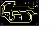
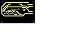
The latest effort, involving most of the easier suggestions in post #1278
I'll work on getting the resistors vertical and making a dual supply version.
Thanks for all the help once more, chaps.
P.S. What size for the Input film cap, C3, 100nF, 1uF?
I'll work on getting the resistors vertical and making a dual supply version.
Thanks for all the help once more, chaps.
P.S. What size for the Input film cap, C3, 100nF, 1uF?
Attachments
That's better. 100 nF wil be OK. BTW you could put footprints over each other giving the possibility to use 2 sizes of for instance connectors and caps. The way you changed the connectors does not make the standard MKDSN fit as the holes are larger. If you rotate R3 90 degrees to the left and change pins 1 and 3 you can make it nicer for R4 and C5 (way shorter track). Q1, D6 and C2 can then move further to the left making it possible to align R5, R6 and R7. C7 and C8 can then also be aligned vertically.
C1 Could be a few mm further from the diode bridge, C2 can move to the left. If you move them both a few mm to the upper side and add an extra footprint for larger filter caps you can experiment or reuse the design for higher voltages/currents.
R1 could be replaced for a coil which has a smaller footprint as it is mounted vertically. If you change the diode bridge for separate diodes you could use Schottky diodes, fast/slow recovery diodes in other words you can use any diode you wish. You could then also add caps parallel to the diodes.
You could also add footprints for a snubber network.
Last edited:
I see what you mean, I will try and refine it some more.
The connectors were just a handy template for soldering wires in, I'm using Diptrace and still trying to find my way around the various connector and component outlines.
For my use it will be with soldered wire but I shall try and find a handy, standard connector for future revisions and put provision in for bare wires/headers too.
Same story for the variable resistor, I happen to have a box various values of trim pot and this footprint seemed to fit what I had, I would be grateful for suggestions as to the best thing to use.
I shall also add footprints for alternative components, I want to add another resistor space in parallel with R1 or perhaps a small inductor for example.
I shall try and shrink it more generally, having the option of board space doesn't mean I have to use all of it I suppose.
Don't solder wires in PCB's. It is old fashioned, meanwhile forbidden according EU rules and making devices prone to failure. It is just cheap, ugly looking and a less good connection. It will damage PCB tracks (which peel off in a breeze anyway with modern material) because of first the soldering and then mechanical strain. It is also a pain to service a device when done so amateurish.
Phoenix MKDSN is THE connector. No steel, no anymetal, just tinned copper/brass. You don't need a special tool for crimping.
Don't just use a potentiometer footprint of one you had in a box for 20 years but add a modern potentiometer footprint over it so you can use both. You may run out of that 20 year old stock and then your PCB is unusable for future PSU's. Bourns 3296 and 3266 are quite standard and the footprint can be used over eachother making it possible to use either one.
BTW this thread is wonderfully derailing into several topics. I don't mind. I just read Elvee is released from the hospital so he likely will join in in this potpourri.
Last edited:
I’m sorry if this is inappropriate for this thread, I shall start another one so as not to add to the confusion.
Could I ask you to move the posts across please?
I wish Elvee the Very best for a speedy recovery, he was very patient with some OT questions I had about some equipment he used on early in this thread.
Thanks for the advice and component names, I shall implement them. 🙂
Could I ask you to move the posts across please?
I wish Elvee the Very best for a speedy recovery, he was very patient with some OT questions I had about some equipment he used on early in this thread.
Thanks for the advice and component names, I shall implement them. 🙂
You can make it available! Just lay it out, order a few dozen boards from your favorite fab, and sell them at whatever price you consider reasonable.
Do it for your comrades. Because you love them!
Do it for your comrades. Because you love them!
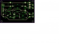
This is the latest, tried to get as man resistors vertical as I could and keep the caps in alignment.
I am trying to keep the traces as short as possible as a point of principle, is placement more important or the former?
I am trying to keep the traces as short as possible as a point of principle, is placement more important or the former?
Attachments
- Home
- Amplifiers
- Power Supplies
- Single sided Denoiser PCB design help