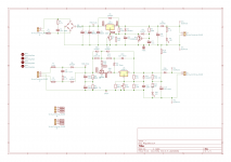
I've built a version of Merlin's Maida HT Regulator + DC heater supply (schematic attached, featured in his hifi book) to power a little PCL82 SE stereo spud amp. I've tried to fit it all in to a small Hammond chassis, with some success. Except for when it's been running for a while...
For the 1st 20 or so minutes, mains hum is practically inaudible. Then it gets distractingly loud. I've yet to take measurements of the ripple or temperature, but the chassis is hot.
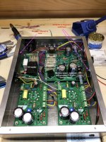
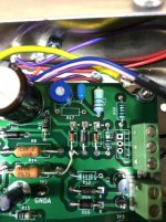
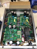
An early version of system had both U1 (an LM317) and Q2 (an IRF820) bolted to the chassis a couple of inches apart as in the attached picture. This was when I noticed the issue first - an intermittent 'put put put'ing every 20 seconds or so when the amp had been running for 20 / 30 mins. Not an oscillation, not at a constant 50 / 100 Hz. This, along with the awful ripple.
Thinking it was a thermal issue, I moved Q2 to the other side of the chassis, thinking the space / surface area might help things. I also then got my own PCBs made up with easier connection points. Replacing all components in the PS and starting afresh, things worked well - until it gets hot...
Would ripple increase if Q2 is overheating? Does this sound a purely thermal problem? Have I massively underestimated the cooling requirements and need to start drilling some air holes in the top?
Numbers:
I estimate the HT is supplying ~55mA at ~280Vdc. Heaters is 0.6A at 14Vdc. Transformer can supply 275-0-275 @ 120mA and 18Vac @3A. Some SPICE simulations indicate the MOSFET is dissipating <2.5W at these operating conditions, but that might be wrong.
I've had success with the same PS design in a preamp supplying 40mA at 280Vdc and 1A at 12Vdc. In this design Q2 had a small heatsink attached to it (venting to inside the chassis) and U1 was chassis mounted.
For the 1st 20 or so minutes, mains hum is practically inaudible. Then it gets distractingly loud. I've yet to take measurements of the ripple or temperature, but the chassis is hot.
An early version of system had both U1 (an LM317) and Q2 (an IRF820) bolted to the chassis a couple of inches apart as in the attached picture. This was when I noticed the issue first - an intermittent 'put put put'ing every 20 seconds or so when the amp had been running for 20 / 30 mins. Not an oscillation, not at a constant 50 / 100 Hz. This, along with the awful ripple.
Thinking it was a thermal issue, I moved Q2 to the other side of the chassis, thinking the space / surface area might help things. I also then got my own PCBs made up with easier connection points. Replacing all components in the PS and starting afresh, things worked well - until it gets hot...
Would ripple increase if Q2 is overheating? Does this sound a purely thermal problem? Have I massively underestimated the cooling requirements and need to start drilling some air holes in the top?
Numbers:
I estimate the HT is supplying ~55mA at ~280Vdc. Heaters is 0.6A at 14Vdc. Transformer can supply 275-0-275 @ 120mA and 18Vac @3A. Some SPICE simulations indicate the MOSFET is dissipating <2.5W at these operating conditions, but that might be wrong.
I've had success with the same PS design in a preamp supplying 40mA at 280Vdc and 1A at 12Vdc. In this design Q2 had a small heatsink attached to it (venting to inside the chassis) and U1 was chassis mounted.
Attachments
The heat produced is a direct result of power dropped across the component. Power equals Voltage times Current.
If you drop 100volts across the FET, it will get hot. You do not state the primary voltages and secondary voltages. The aim is to drop a minimal voltage, giving enough voltage drop to absorb any ripples.
Why are your heaters at 1/3rd HT? That will cause leaks within the valves.
DC heaters should not be elevated.
Last edited:
Thanks - I'll run through the design calcs:
240 primary, 275-0-275 secondaries for the HT
RMS / peak AC conversion: 275 * 1.35 = 371 Vrms
Allow 5% reduction in mains: 371/1.05 = 353.6 Vrms
Rectifier drops: 353.6 - 1.4 = 352.2 Vdc
Min 10V MOSFET valleys drop: 352.2 - 10 = 342.2 Vdc
Regulator 20V drop: 342.2 - 20 = 322.2 Vdc
Protection diode drop: 342.2 - 0.7 = 321.5 Vdc
I'm aiming for 280Vdc, so need to drop ~ 10 + 20 + 40 = 50V across the MOSFET Q2 & regulator U2, at 0.055mA, so ~ 4W dissipation. I'd thought chassis mounting Q2 could dissipate this...
As it's adjustable I could just go for a higher HT keeping an eye on the max dissipation in the PCL82. My SPICE simulations indicate the rapid increase in power dissipated when keeping the output load somewhere on the intended load line.
As for the elevated DC heaters - I was just following others. Will have to read-up on this...
Attachments
Last edited:
I'm aiming for 280Vdc, so need to drop ~ 10 + 20 + 40 = 50V across the MOSFET Q2 & regulator U2, at 0.055mA, so ~ 4W dissipation. I'd thought chassis mounting Q2 could dissipate this...
On the heat sink, I was working on the following for Q2:
P = (Vin - Vout - 12) x Iout
P = (352 - 300 - 12) X 0.055
P = 2.2W
Allowing a 60deg temp rise:
R_sink = 60 / P - 3
R_sink = 24 C/W
Which is achievable using a flat-plate calculator and assuming one face of my chassis is the plate: Free Flat Plate Heat Sink Calculator
P = 2.2W
Allowing a 60deg temp rise:
R_sink = 60 / P - 3
R_sink = 24 C/W
So I might have been a bit off in the power & R_sink calcs. I'll take actual measurements tonight, but modelling gives just under 5W dissipation in the MOSFET. And a slightly bigger sink at 3.2 C/W to keep things well under the 150deg max junction temperature.
If my MOSFET was overheating, derating and losing the ability to control the current, that could explain the increase in hum when running for longer periods?
Next steps are to
- take a few measurements to confirm the voltage drops / current
- fit a small BGA sink on the IRF820 case
- add some air holes to the top and bottom of the chassis
- add a larger heatsink to the outside of the chassis, with a bolt connecting through the to the MOSFET & a thermal pad inbetween.
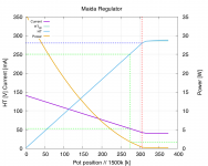
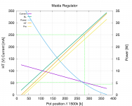
Attached is an updated graph showing how the power dissipated in the MOSFET varies with pot adjustment. The orange line marked HT is the voltage connected to the PCL82 pentode, and the purple line is current flowing based on the loadline calculated at a 250V operating point.
What I hadn't realised was that increasing the HT value obviously changes the load line position, increasing the current too. Whilst this chart suggests increasing the HT lowers the power dissipated. But that is clearly wrong when the load is taken in to account - I'd need to vary the bias too. If anything, I'm running these PCL82s on the edge of the safe region at 250V, so the heat sinking will be required!
Attachments
Magic smoke... What to replace?
I tried to take some measurements the other evening and the following happened:
Merlin billed this PS as almost indestructible, so I consider this an achievement!
Switching it off as fast as I could, I then did a few checks & saw nothing untoward, turned the pot back the to where it was (or maybe I didn't...) Turning the amp back on there was a little more smoke, sound still being produced, as the output voltage dropped from ~330V down to ~40V at which point sound stopped and I powered down. The result is attached.
The fried resistor is R11 which works in conjunction with D13 & the LM317L to protect the MOSFET, I believe.
I'll replace R11 (obviously) & RV2 in case its tracks are fried. Would there be other contenders?
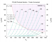
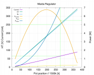
Also attached is a better simulation of what's going on - the triodes and pentodes are included in the SPICE model. This shows I'm running right on the PCL82 dissipation limit of 7W, the MOSFET is dissipating 5.5W and the pot is dissipating <0.5W.
I tried to take some measurements the other evening and the following happened:
- I turned the pot RV2 down probably a little too fast
- I started to hear cracking / seeing little flashes around the pads for Q2, R10 and below RV2
- some bad smoke started rising...
Merlin billed this PS as almost indestructible, so I consider this an achievement!
Switching it off as fast as I could, I then did a few checks & saw nothing untoward, turned the pot back the to where it was (or maybe I didn't...) Turning the amp back on there was a little more smoke, sound still being produced, as the output voltage dropped from ~330V down to ~40V at which point sound stopped and I powered down. The result is attached.
The fried resistor is R11 which works in conjunction with D13 & the LM317L to protect the MOSFET, I believe.
I'll replace R11 (obviously) & RV2 in case its tracks are fried. Would there be other contenders?
Also attached is a better simulation of what's going on - the triodes and pentodes are included in the SPICE model. This shows I'm running right on the PCL82 dissipation limit of 7W, the MOSFET is dissipating 5.5W and the pot is dissipating <0.5W.
Attachments
Famous last words... I think this may be related to a problem identified on my erratum page:Merlin billed this PS as almost indestructible,
In fig. 11.48 a possible failure mechanism exists if the output voltage is turned all the way down with no load. This is due to the 317L not being able to sink the current through R1+R2+D1. A known fix is to increase R1 and R2 by a factor of 10 (e.g. 1Meg and 82k). Thanks to Menno van Der Veen for pointing this out.
http://valvewizard.co.uk/Book3.html
Thanks Merlin.
In my case I turned the pot down prior to the heaters warming up, therefore no load / current flowing. Makes sense.
Will make those changes / replace the likely fried components and attach a beefier heat sink. Then to chase down why the hum increases with reduced voltage.
In my case I turned the pot down prior to the heaters warming up, therefore no load / current flowing. Makes sense.
Will make those changes / replace the likely fried components and attach a beefier heat sink. Then to chase down why the hum increases with reduced voltage.
Found an error on my board... Have blown quite a few iRF820s and LM317Ls to get to this point! So obvious in hindsight; wrong diode D11 connection which throws all the voltages and, I guess, damages a few components here and there... Awaiting replacement components to re-do the regulator post-Christmas.
Will report back...
Will report back...
Can you explain the "wrong connection" a little better? Like, installed wrong-way-round, or just between the wrong points?
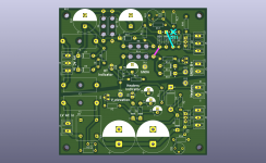
Wrong points... A combination of transcribing the circuit from Merlin's book / PDF incorrectly and having the grid in KiCad too fine. So not only did a net not connect to where it should (minuscule gap between D12/D13 and R12 on the schematic, jumper pink line in attached), but I had a diode D11 connect to wrong side of R11 (new location in blue).
And I don't know what other components on the HV regulator side I may have fried by firing it up for testing. So probably easier to start afresh.
Interestingly (to me), D11 being wrongly connected meant the voltage could not be lowered any further than ~280V when adjusting the pot. This is exactly what happened when I tested - and me adjusting it lower is when it went pop. A LTSPICE sim confirms this behaviour but doesn't seem to indicate what component might have dissipated too much energy.
Attachments
The heat produced is a direct result of power dropped across the component. Power equals Voltage times Current.
If you drop 100volts across the FET, it will get hot.
Instead of the two fuses on the HT, use power resistors in their place, or keep the fuses and one bigger power resistor ahead of the feed point for the MOSFET and LM317. 1.5k@10W will drop the voltage ~83V
Or a bigger heat sink -- 100V 55mA -- 5.5W, to be on the safe side something like an Aavid Thermalloy HS374.
On your PCB place a "keep-in:keep out" layer between the HV and ground, or cut a slot between the HT and ground.
Last edited:
This is what I've tried - I bought a 40mm square finned heat sink, drilled a hole in the center, and mounted it to the outside of the chassis with thermally conductive insulating material between. The MOSFET is bolted to this through the chassis, with a sil pad / top hat for insulation. If I can get the damn thing to operate again we'll see if this is sufficient.Or a bigger heat sink -- 100V 55mA -- 5.5W, to be on the safe side something like an Aavid Thermalloy HS374.
The original problem was an increase in hum as I turned down the Vout. This could have been due to the MOSFET over heating? ie, derating itself as its temperature increases. So if I keep it cooler hopefully this will be solved.
I don't quite follow. The upper region of the PCB is the HV side - the copper pour is GND. The lower region is the LV side - the copper pour here is referenced to an elevated voltage via R19 or linked to GND with a jumper. I increased the DRC clearances / keep-outs to what looked sensible and kept the pour to the top side.On your PCB place a "keep-in:keep out" layer between the HV and ground, or cut a slot between the HT and ground.
A quick update - I found another inexcusable error on my pcb which, when simulated, explained much of the recent behaviour. That is now fixed.
Pleased to report I have a working system after spinning another set of boards + some additions. Reading Pease's book on troubleshooting analogue circuits enforced the possibility that the MOSFET could have been oscillating, so I moved the stoppers from the main board to a little break-out board I had made to house the FET. This means the FET can be moved to the heatsink.
The addition of the two heatsinks (for the HV MOSFET and LV regulator) have made the chassis a more sensible temperature.
My original issues (put put putting noise and some hum when warmed up) seem to have been resolved - so perhaps they were a combination of oscillation and / or over-heating.
This build is now sitting in my kitchen attached to a Pi Zero through a miniDIN umbilical - supplying 5V, GND, amp on/off signal from a GPIO pin, L, R & audio ground. Works fairly well as a kitchen radio, but more tweaking likely.
Attachments
For the benefit of anyone in the future looking at this, I've placed all the source files (KiCAD) and gerbers for this Maida Regulator board here: amps/HiFi-MaidaRegulator at master * tristancollins/amps * GitHub
Along with the little breakout boards:
amps/General-MOSFET-Breakout at master * tristancollins/amps * GitHub
amps/General-TO220-Breakout at master * tristancollins/amps * GitHub
Along with the little breakout boards:
amps/General-MOSFET-Breakout at master * tristancollins/amps * GitHub
amps/General-TO220-Breakout at master * tristancollins/amps * GitHub
- Status
- This old topic is closed. If you want to reopen this topic, contact a moderator using the "Report Post" button.
- Home
- Amplifiers
- Power Supplies
- Symptoms of overheating - Maida Regulator