I'm designing a replacement capacitor board for the Adcom GFA-535 and 545, and I want to make sure this board is optimized for low noise. Do you see any issues with this layout? I'm not sure I'm considering the various currents properly. It's a surprisingly complex issue. I've based the layout on the originals boards, but since I'm stuffing larger drain resistors and bypass caps on it, the layout has to change to 2-layer.
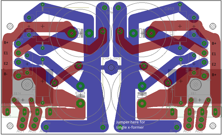
In the diagram, E1 is the zobel, and E2 is the signal ground.
There are several reasons for the new boards. For one thing, I see burned out bridge rectifiers on these amps sometimes. As a part of my refurbishing service, I attach heatsinks to new, higher-current bridge rectifiers. A better solution is to mount the bridge to the chassis, so this board puts it on the bottom of the board. Also, the old capacitors are 4-pin, 22mm LS types and they can't be found anymore. I've been spending a lot of time converting the boards to accept 10mm LS capacitors.
You can download the Eagle file here...
https://www.dropbox.com/s/0hdndu7jcabjylx/Capacitor Board.brd?dl=0
Any help is appreciated!
Last edited:
I'm designing a replacement capacitor board for the Adcom GFA-535 and 545,
and I want to make sure this board is optimized for low noise.
I think we should start over. Can you post the schematic as a PDF, and the BOM?
Sure, here's the service manual.
https://www.dropbox.com/s/dio6e1zsy54lbmx/hfe_adcom_gfa-545_ii_service.pdf?dl=0
https://www.dropbox.com/s/dio6e1zsy54lbmx/hfe_adcom_gfa-545_ii_service.pdf?dl=0
Sure, here's the service manual.
Ok, are the rectifier terminals soldered to the board? They are fast-on terminals.
Is the board mounted with 5 screws?
Last edited:
Yes, there are five screws. The center is chassis ground. The bridges mount below the board, screwed to the chassis through the 6.3mm holes in the boards, their leads bent upwards into through-holes in the board. Outlines of the bridges are shown by the grey boxes.
Last edited:
Yes, there are five screws.
Ok, first try to place the bridges, [and capacitors as you have], symmetrically
on the board wrt the ground bolt. Also make the board edges symmetric around
the 4 large capacitors. The manual appears to show the pcb that way.
Post just this layout.
Last edited:
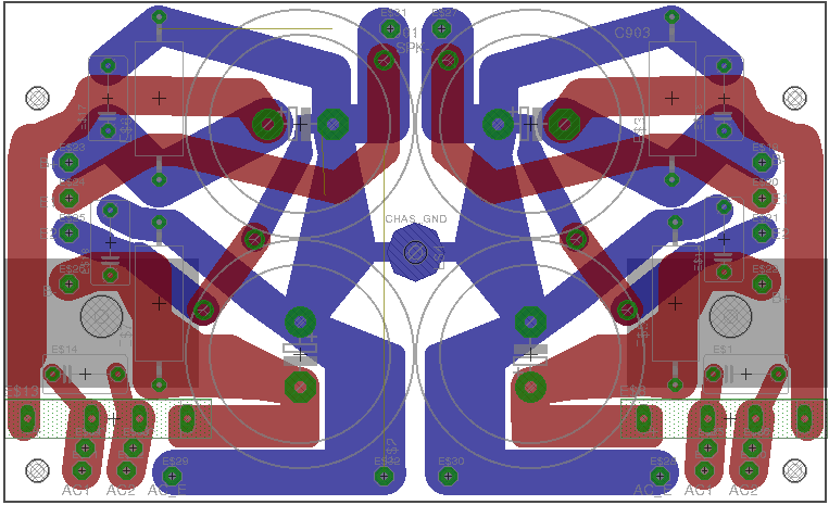
OK, I think this is better...
I read a few articles on the subject, such as this one which was particularly helpful.
http://www.geofex.com/article_folders/stargnd/stargnd.htm
...and taking inspiration from how amps like the GFA-565 are wired, I've come up with this, which I'm pretty sure it's optimal. The rectifier currrents now folllow a separate path from the signal ground, which is taken right off the top filter cap. E2 is just for Zobel, so it's placed next to the speaker ground. Chassis ground location shouldn't matter much, it only conducts shielding current.
This might even be a little better than stock. In the original layout, it seems to me that current flowing between the bottom capacitor and the speakers could modulate the signal ground. (Signal ground is E3 and E4 on the Adcom board and E2 on mine)
OK, I think this is better...
This shows the rectifiers as a vertical package. Which one is correct.
OK, I think this is better...
Really? That looks like one bad Eagle layout.
 We all have to start somewhere though.
I've got several 535II's and they all have vertical 4 lead rectifiers on top of the capacitor boards. There are no bent leads that you're referring to.
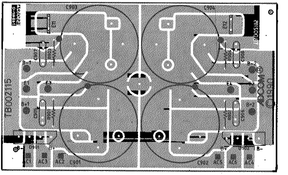
Why don't you copy the factory board as close as possible?
What are you trying to improve upon with your own board?
Just visited your site phloodpants.
You describe the board pictured below as having "plated through-holes".
It looks to me like the pads are ONLY on the bottom layer, instead of being on the top and bottom layers like shown in this image:
https://cdn.sparkfun.com/assets/b/2/a/f/d/50d4b1fcce395f8655000000.jpg
In the end and when all the dust settles, it's all about keeping those good ole' Adcom amps. alive.
Keep up the great work!
Attachments
Thanks, yes actually my GFA-565 boards do have plated through-holes; they just don't have pads on top. There is a metal tube in each hole. This is a more solid and physically strong connection than the original boards that were just ordinary single-side boards.
Just visited your site phloodpants.
You describe the board pictured below as having "plated through-holes".
It looks to me like the pads are ONLY on the bottom layer, instead of being on the top and bottom layers like shown in this image:
https://cdn.sparkfun.com/assets/b/2/a/f/d/50d4b1fcce395f8655000000.jpg
In the end and when all the dust settles, it's all about keeping those good ole' Adcom amps. alive.
Keep up the great work!
Really? That looks like one bad Eagle layout.
I've got several 535II's and they all have vertical 4 lead rectifiers on top of the capacitor boards. There are no bent leads that you're referring to.
Why don't you copy the factory board as close as possible?
What are you trying to improve upon with your own board?
What makes it a bad layout? Be specific.
There are several reasons for me doing this, as outlined in the original post.
1. To fit larger drain resistors and bypass capacitors.
2. To add a snubber cap across the AC terminals of the bridge
3. I want to mount the bridge rectifier to the chassis for better cooling. That is why I am bending the leads.
4. They don't make 22mm lead-spacing capacitors anymore.
Thanks, yes actually my GFA-565 boards do have plated through-holes; they just don't have pads on top. There is a metal tube in each hole. This is a more solid and physically strong connection than the original boards that were just ordinary single-side boards.
If your boards don't have the pads on top as well as the bottom for axial leaded components, then it's not the same.
Perhaps in your eyes, if those "metal tubes" makes a big difference, that's all that matters.
All boards I lay out have pads on both sides for a truly "more solid and physically strong connection" for all axial leaded parts.
What makes it a bad layout? Be specific.
"Looks" is the key word in my post. Hey, if you think your layout looks great and will work great, that's all that matters.
3. If you've determined that the factory rectifiers are crap, run hot and just not up to the job, why not just get some KBPC5010 50A 1KV jobs and "bolt them to the chassis"? No lead bending required. Be sure and run some 10awg OFC wire to them.
That ought to "Get-R-Done"!
- Status
- This old topic is closed. If you want to reopen this topic, contact a moderator using the "Report Post" button.
- Home
- Amplifiers
- Power Supplies
- Critique my capacitor board for Adcom GFA-535/545