First order capacitance multipliers (the ones that rely simply on the h22 of the active device and not on additional FB loops) are limited in their ultimate rejection level, mainly because of the finite output impedance of the active element.
This impedance stems from the Early effect (for BJT's).
The Early effect modulates the Hfe as a function of Vce, and as a consequence the necessary base current for a certain Ic, which in turn modulates the Vbe, causing non-infinite rejection of the ripple towards the output.
To combat that effect without resorting to additional feedback loops, various strategies are possible.
Here is an example:
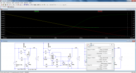
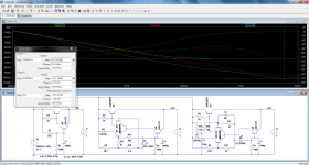
The first pic shows a plain-vanilla, CFP-based capacitance multiplier.
We can see that the rejection bottoms at ~-62dB (green trace). This value is typical for this type of circuit.
A strategy to compensate for the effect would be to modulate the base current of the pass element, so that the apparent Hfe becomes constant.
That's what the circuit on the right does: Q7 and Q6 form a modulator, with the current to be modulated entering the emitters and the modulating signal being applied to the bases. Because of R10 and R8, Q7 receives an image of the drop-out voltage and corrects the current sent to Q6's base accordingly.
To reduce the waste current dumped by Q7, an additional offset introduced by R12.
The arrangement also has the side benefit of cascoding Q8, and thus eliminating the Early effect at its level.
The result (red trace) is a substantial improvement in possible rejection: 34dB
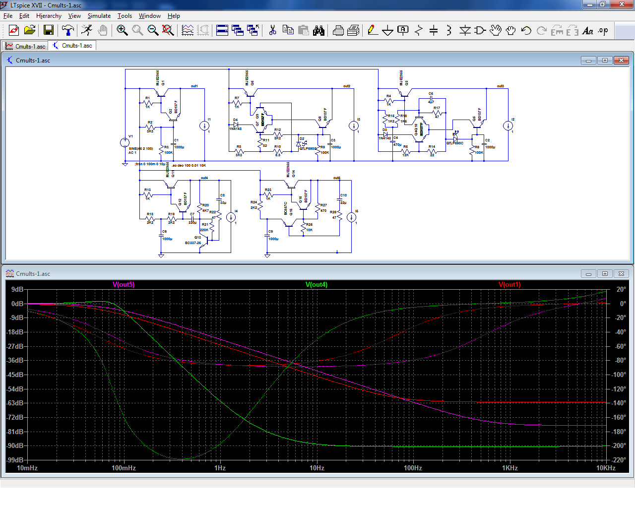
The third variant uses the same principles, but implemented differently, using a partial two-pole filtering, giving further improvements in the LF region, and yielding an ultimate rejection >100dB.
The circuits shown are conceptual ones, with all the usual accessories removed for the sake of clarity. A real implementation should of course include those.
This impedance stems from the Early effect (for BJT's).
The Early effect modulates the Hfe as a function of Vce, and as a consequence the necessary base current for a certain Ic, which in turn modulates the Vbe, causing non-infinite rejection of the ripple towards the output.
To combat that effect without resorting to additional feedback loops, various strategies are possible.
Here is an example:
The first pic shows a plain-vanilla, CFP-based capacitance multiplier.
We can see that the rejection bottoms at ~-62dB (green trace). This value is typical for this type of circuit.
A strategy to compensate for the effect would be to modulate the base current of the pass element, so that the apparent Hfe becomes constant.
That's what the circuit on the right does: Q7 and Q6 form a modulator, with the current to be modulated entering the emitters and the modulating signal being applied to the bases. Because of R10 and R8, Q7 receives an image of the drop-out voltage and corrects the current sent to Q6's base accordingly.
To reduce the waste current dumped by Q7, an additional offset introduced by R12.
The arrangement also has the side benefit of cascoding Q8, and thus eliminating the Early effect at its level.
The result (red trace) is a substantial improvement in possible rejection: 34dB
The third variant uses the same principles, but implemented differently, using a partial two-pole filtering, giving further improvements in the LF region, and yielding an ultimate rejection >100dB.
The circuits shown are conceptual ones, with all the usual accessories removed for the sake of clarity. A real implementation should of course include those.
Attachments
The current through the LED is less than half a mA, so its dynamic impedance (dV/dI) might not be low. This makes me a bit concerned that the base of Q9 is not driven stiffly; I worry that a transient step-change in the load current I3 (especially, a step from 1.0A to 0.1A in 100 nsec) might cause overshoot at the base of Q6.
It is a proof-of-concept circuit, not something that is intended to be actually built in this form, and I didn't look after practical details.The current through the LED is less than half a mA, so its dynamic impedance (dV/dI) might not be low. This makes me a bit concerned that the base of Q9 is not driven stiffly; I worry that a transient step-change in the load current I3 (especially, a step from 1.0A to 0.1A in 100 nsec) might cause overshoot at the base of Q6.
I chose a LED because it was simple and quick, but that wouldn't be my choice for a real circuit anyway because the dropped voltage is uselessy high.
The candidate-builder has to work out for himself the issues like bias current, possible bypassing of the LED or diodes, etc according to his requirements
Here is an example of Denoizator fitted to a capacitance multiplier, following a suggestion by Sgrossklass (the two bottom circuits):
Other CapMult improvement examples can be found here:
https://www.diyaudio.com/forums/pow...s.html?highlight=capacitance+multiplier+early
Other CapMult improvement examples can be found here:
https://www.diyaudio.com/forums/pow...s.html?highlight=capacitance+multiplier+early
Attachments
Last edited:
- Status
- This old topic is closed. If you want to reopen this topic, contact a moderator using the "Report Post" button.