Hi,
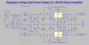
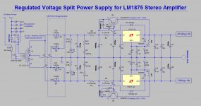
Here is the circuit diagram for LM1875 stereo amplifier build power supply. Suggestions and improvements are welcome.
Please, check out the polarity of the MJE2955 transistors (used across each positive and negative supply rails) in this split power supply design with 25-0-25 volts center tap transformer. Did i implemented the use of MJE2955 correctly?
Plz, Check out the RC's. if they are done/implemented the right way.
I will be using the 8ohms speaker each for left and right channel, with this power supply for LM1875 stereo amplifier design.
LM/LT 317 and LM/LT 337 regulators are used for positive and negative rails respectively. MJE2955 (PNP Transistor) is used for increasing the current capacity of the circuit up to 5 Ampere, at least. KBPC3510 Bridge (that's what is easily and only available here) is used for rectification.
Combination of 2200uf and 10,000uf is used as a smoothing tank reservoir.
Will this power supply work best? Is everything OK in the schematic? Sorry! i don't have power supply testing instruments with me. So, this is only a conceptual schematic. No measurements are performed, yet. Is there any other possible design better than this for LM1875 stereo Amp. build? Is there any other modification required to make this power supply perform even better, with noise figures, distortions, sound sonics and sound clearity?
Thanks.
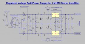
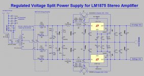
Attachments
Last edited:
Your LED's are backward.
I think you are talking about polarity? If yes than, thanks, i will invert the LED symbol in the schematic.
Thanks
C35 non-polarized 47000uF@400V may be an unpractical component.
C35 is not 47000uf@400V. It is .047uf/400V which is equivalent to 47000 pico farad which is equivalent to 47 nano farad and who's EIA code is 473.
Thanks.
The transistor in the negative rail should be an NPN. What does your SIM show? The -25V should be ok, but no current/power in that PNP.
Thanks!. This is really i was confused about. So i asked, to check the polarity and implementation of Q1 and Q2 transistors. Actually, this is first time i am creating a split rail power supply. With single supply i know how to use NPN as well as PNP. But, i had no idea and experience about the negative rail transistor, its type and polarity.
So, i think now i conclude that the opposite type pair goes together in a split supply?
If i use NPN in positive rail then i have to use PNP in a negative rail and if i use PNP in a positive rail then i have to use a NPN in a negative rail with Center tap traffo. Am i right?
However, with dual secondary supply traffo, The case is different. We can use both PNP. With dual supply traffo, the negative wire of one supply is shorted with the positive wire of another supply, thus forming the center ground and we can then use both transistors as PNP.
Am i all right about this? Will this all goes this way?
I have not build the power supply practically yet. Once, the design will be final and approved by here at diyaudio members, I will then go for an actual implementation.
I think the new design will be as such:
Thanks.
Attachments
Last edited:
What the hell is a Farad
C35 is shown as .047/400V. When a capacitor value prefix
is not otherwise indicated as in uF, nF, pF, it is assumed that the no prefix
value is in Farads (F). LTspice certainly assumes this.
The reactance of your newly invented C35/ .047uF capacitor is
over 50Kohms at 60 Hz. Your supply will not work. I know you
have not run a simulation with load, successfully.
You will probably wish the value was 47000uF to get anything
to work properly under load.
Presenting a schematic with bogus values requiring us to read
your mind is a silly endeavor. Clean up your schematic !!!
C35 is not 47000uf@400V. It is .047uf/400V which is equivalent to 47000 pico farad which is equivalent to 47 nano farad and who's EIA code is 473.
Thanks.
C35 is shown as .047/400V. When a capacitor value prefix
is not otherwise indicated as in uF, nF, pF, it is assumed that the no prefix
value is in Farads (F). LTspice certainly assumes this.
The reactance of your newly invented C35/ .047uF capacitor is
over 50Kohms at 60 Hz. Your supply will not work. I know you
have not run a simulation with load, successfully.
You will probably wish the value was 47000uF to get anything
to work properly under load.
Presenting a schematic with bogus values requiring us to read
your mind is a silly endeavor. Clean up your schematic !!!
You do not want 47nF in series with your primary.
But somebody asked me to: Add some MOV's or an AC rated polyester cap or RC at transformer Primary.
What does this really means? How can i implement the same and with what values?
Thanks.
C35 is shown as .047/400V. When a capacitor value prefix
is not otherwise indicated as in uF, nF, pF, it is assumed that the no prefix
value is in Farads (F). LTspice certainly assumes this.
I agree 100%. And, my apologies for forgetting to show "uf" in the schematic. Please, check out, I rectified the mistake in the last diagram.
The reactance of your newly invented C35/ .047uF capacitor is
over 50Kohms at 60 Hz. Your supply will not work. I know you
have not run a simulation with load, successfully.
Actually, i wanted to, Add some MOV's or an AC rated polyester cap or RC at transformer Primary. But i don't know how to do this and with what proper values. So, i end up using .047uf/400v AC cap at primary input, which is actually an X capacitor connect in parallel to the mains(parallel to power on off switch primarily). Offcourse, power supply won't work until this cap is bypassed or the power on/off switch is in ON position.
Can you tell me how to Add some MOV's or an AC rated polyester cap or RC at transformer Primary, and with what proper values in my design?
Thanks.
Last edited:
1. LED D9 is mounted wrong. Should flip vertically;Thanks!. This is really i was confused about. So i asked, to check the polarity and implementation of Q1 and Q2 transistors. Actually, this is first time i am creating a split rail power supply. With single supply i know how to use NPN as well as PNP. But, i had no idea and experience about the negative rail transistor, its type and polarity.
So, i think now i conclude that the opposite type pair goes together in a split supply?
If i use NPN in positive rail then i have to use PNP in a negative rail and if i use PNP in a positive rail then i have to use a NPN in a negative rail with Center tap traffo. Am i right?
However, with dual secondary supply traffo, The case is different. We can use both PNP. With dual supply traffo, the negative wire of one supply is shorted with the positive wire of another supply, thus forming the center ground and we can then use both transistors as PNP.
Am i all right about this? Will this all goes this way?
I have not build the power supply practically yet. Once, the design will be final and approved by here at diyaudio members, I will then go for an actual implementation.
I think the new design will be as such:
Thanks.
2. R10 and R11 values are rather small. Assuming 35Vdc potential for one LED about 5mA, then each resistors should be about 7K;
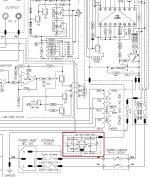
3. R1, C31, or R3, C32 is just a fad, especially as talk of a power supply whose frequency is 50/60Hz. I recommend you give up that's snubber and then you can use in the primary side of the transformer more useful circuit (see the circled in red in the attached picture below);
4. Should you give up R2 and R4. If you quit mount these resistors, then you can quit and C1 and C2.
5. The output LT317/337 should be connected ballast resistor, which is especially useful when you want to test power suplly at no load operation (ie without connecting power amplifiers). This resistor is dimensioned for the lowest current which are provided to stabilize performance, typically 10mA. For example, 25Vdc, you need a resistor 2k2 - 1W.
6. In parallel with the BE junction of Q1 and Q2, I recommend you install two diodes in series, type 1N4007.
7. If you want, you could implement the Slow Turn-On as recommended in the LM317 datasheet, see page 16 from here.
8. C23 ... 26's better to be 22nF or 47nF.
9. C21 and C22 should be of greater capacity, for example 1000uF.
10. Diodes D3 and D4 should be moved in parallel with the collector and emitter terminals of the transistors Q1 and Q2. In this case, instead of 1N4007 should use something like BY255 or 1N5404.
These would be the most important observations should be aware.
Attachments
Let's not confuse you!
You have drawn a schematic with a really big 0.047F cap in series with the primary. In fact there are (few) diyers who do something like that. They want to avoid DC current from the mains to saturate the primary of the transformer. A practical solution has eben presented to you by donpetru. If you ask me, save that idea for later.
Add an X capacitor to the primary. Just connect it in parallel with the primary. Yes, there will be mains voltage across the cap all the time as Long as the amp is on. That's why it has to be a special type of capacitor. Look out for an X2. 47nf is a reasonable value. What does it do? It Shorts out some high frequency noise from the mains and/or your amp. And: Even when your amp is idle there is some (magnetizing) current flowing through the primary. This current is limited by the prim. inductance. When the AC switch is opened the X capacitor gives the induktive current a path and thus avoids inductive peaking. Good for the switch, and no switch-off-popp.
Thanks! for the reply Mr.donpetru.
The attached picture by you, shows the circuit attached in series with the mains neutral terminal. It consists of a KBPC 352 bridge and four electrolytic capacitors(4700uf/6.3v). Can we use diodes in place of a bridge and 4700uf/25v electrolytic capacitors instead of 6.3v capacitors?
I want to use at least one CRC network in this power supply. Giving up R2 and R4 will totally defeat the purpose.
Let me see if i can get a 2.2k - 1w Ballast resistor, here at the shop. I save this idea for later.
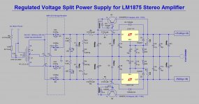
Done! Please check if its implemented the right way. Specially check the polarity of diodes at each positive and negative rail.
What are the actuall benefits of Slow Turn-On?
If i opt to use Slow Turn-On implementation, does that imply that i won't be requiring, extra "speaker saving on/off relay circuit", at the amplifiers output stage during power supply on and off?
Actually, I want to save it for later once when the Amplifier will be up and running and i feel the need to do so.
Rest all points are check and done. Please verify them in the newly updated schematic here:
Thanks.
The attached picture by you, shows the circuit attached in series with the mains neutral terminal. It consists of a KBPC 352 bridge and four electrolytic capacitors(4700uf/6.3v). Can we use diodes in place of a bridge and 4700uf/25v electrolytic capacitors instead of 6.3v capacitors?
4. Should you give up R2 and R4. If you quit mount these resistors, then you can quit and C1 and C2.
I want to use at least one CRC network in this power supply. Giving up R2 and R4 will totally defeat the purpose.
5. The output LT317/337 should be connected ballast resistor, which is especially useful when you want to test power suplly at no load operation (ie without connecting power amplifiers). This resistor is dimensioned for the lowest current which are provided to stabilize performance, typically 10mA. For example, 25Vdc, you need a resistor 2k2 - 1W.
Let me see if i can get a 2.2k - 1w Ballast resistor, here at the shop. I save this idea for later.
6. In parallel with the BE junction of Q1 and Q2, I recommend you install two diodes in series, type 1N4007.
Done! Please check if its implemented the right way. Specially check the polarity of diodes at each positive and negative rail.
7. If you want, you could implement the Slow Turn-On as recommended in the LM317 datasheet, see page 16 from here.
What are the actuall benefits of Slow Turn-On?
If i opt to use Slow Turn-On implementation, does that imply that i won't be requiring, extra "speaker saving on/off relay circuit", at the amplifiers output stage during power supply on and off?
Actually, I want to save it for later once when the Amplifier will be up and running and i feel the need to do so.
Rest all points are check and done. Please verify them in the newly updated schematic here:
Thanks.
Attachments
Last edited:
Thanks! Mr.grommeteer,
Its done! please check out the last schematic.
Thanks.
Add an X capacitor to the primary. Just connect it in parallel with the primary.
Its done! please check out the last schematic.
Thanks.
Diodes D11, D12, D13, D14, must be connected backwards because you did not properly connected.
Then, should give up resistance of 3.3 Ohm 10W and apply my instructions from the point no.3 above.
Slow Turn On option will not eliminate the need for a relay on each amplifier output but will bring a slight improvement of the amplifier power supply.
Then, should give up resistance of 3.3 Ohm 10W and apply my instructions from the point no.3 above.
Slow Turn On option will not eliminate the need for a relay on each amplifier output but will bring a slight improvement of the amplifier power supply.
The CRC filter R2 & R4 is unnessary. It only serves to reduce the voltage headroom that the active regulator has to work with.
I would also remove C5, C6, C7, C9, C13, C15, C17 & C18. These only serve to keep the LM3XX regulators and the series pass transistors from reacting to load induced voltage fluctations. The effect of this is to increase the output impedance of the supply at higher frequency. Try similating this with an active load of a current source offset at desired load current and a 1K sign wave, then remove those Cs and watch the voltage at the output smooth out. The higher the frequency the more load induced ripple you will get with those caps in place.
I would also remove C5, C6, C7, C9, C13, C15, C17 & C18. These only serve to keep the LM3XX regulators and the series pass transistors from reacting to load induced voltage fluctations. The effect of this is to increase the output impedance of the supply at higher frequency. Try similating this with an active load of a current source offset at desired load current and a 1K sign wave, then remove those Cs and watch the voltage at the output smooth out. The higher the frequency the more load induced ripple you will get with those caps in place.
I corrected the above diagram.
It would be better to use two transistors MJE2955 in parallel and two 2N3055 in parallel. In this case PSU will be more reliable. Or you could try to use MJ15024 / MJ15025. I know there are more expensive but higher power.
It would be better to use two transistors MJE2955 in parallel and two 2N3055 in parallel. In this case PSU will be more reliable. Or you could try to use MJ15024 / MJ15025. I know there are more expensive but higher power.
Attachments
- Status
- This old topic is closed. If you want to reopen this topic, contact a moderator using the "Report Post" button.
- Home
- Amplifiers
- Power Supplies
- Regulated Power supply design suggestions and updates for LM1875 stereo amplifier