Hey there,
I posted here due to the focus of my question being around the MPSA13, J111, J174, and M5201 components of the switching circuit of this amp. Apologies in advance if I got it wrong.
I own this amp and what drew me to the circuit initially was that my channel A reverb was not working. I carried out various voltage tests and eventually after touching up some joints I now have channel A reverb. What bugs me is some things did not seem to add up when voltage testing.
For example: I understand that the M5201 should switch between its op amps when voltage is applied to pin one, ctrl pin. However, when I test for voltage at that point, I have a constant 30vdc at pin one on IC8 when depressing both the footswitch button and the panel switch (the channel is audibly changing from clean to crunch).
Also, can someone give a layman's account of what is actually happening in the 'switching circuit', and what TR 1, 2, and 3 actually do?
What bothers me is, if IC7 is responsible for selecting which channel's reverb is on, why is the control voltage not changing? When/how/why does the channel change and the reverb change over?
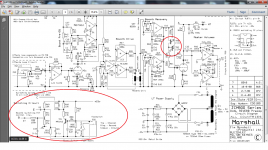
Schematic detail attached,
Thanks a lot
Imgur: The magic of the Internet
https://i.imgur.com/GnL5jSv.png
I posted here due to the focus of my question being around the MPSA13, J111, J174, and M5201 components of the switching circuit of this amp. Apologies in advance if I got it wrong.
I own this amp and what drew me to the circuit initially was that my channel A reverb was not working. I carried out various voltage tests and eventually after touching up some joints I now have channel A reverb. What bugs me is some things did not seem to add up when voltage testing.
For example: I understand that the M5201 should switch between its op amps when voltage is applied to pin one, ctrl pin. However, when I test for voltage at that point, I have a constant 30vdc at pin one on IC8 when depressing both the footswitch button and the panel switch (the channel is audibly changing from clean to crunch).
Also, can someone give a layman's account of what is actually happening in the 'switching circuit', and what TR 1, 2, and 3 actually do?
What bothers me is, if IC7 is responsible for selecting which channel's reverb is on, why is the control voltage not changing? When/how/why does the channel change and the reverb change over?
Schematic detail attached,
Thanks a lot
Imgur: The magic of the Internet
https://i.imgur.com/GnL5jSv.png
Last edited:
C20 is held at +15
When the switch closes its contact on the foot pedal, the voltage on C20 collapses causing low voltage on D6 & D7.
D7 pulls point B negative causing TR3 to conduct, passing signal.
Point E is allowed to float due to D6 no longer conducting causing TR2 to become high resistance and allows the signal to flow.
When the switch is off, C20 goes high, switching TR2 on, that shunts the signal and TR3 is switched off, and no longer conducts.
A basic TTL array.
This has no effect on the ICs it just controls the signal.
Last edited:
Great thanks for that comprehensive answer. As someone not too familiar with solid state, it's going to take me some time to get my head around it, however I will persist. Thank you for the explanation.
Should I assume then, when reverb is on via the footswitch, that both reverbs are on simultaneously i.e, it doesn't actually 'flip/flop' from one half of IC7 to the other?
I'm still not really clear how the amp is changing channels, i.e, between IC8 a and b, when there is a constant voltage on pin 1 of IC8 regardless of whether the amp is in channel A or B. Or is it that the current is changing?
Last edited:
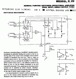
M5201 datasheet mentions current in or lack of it for 2 possible states.
Voltage may very well be the same.
As a side note, you can´t have 30V anywhere around there, Op Amp is fed +/-15V and switcher is fed +15V
Voltage is always measured relative to ground, unñess otherwise noted.
Voltage may very well be the same.
As a side note, you can´t have 30V anywhere around there, Op Amp is fed +/-15V and switcher is fed +15V
Voltage is always measured relative to ground, unñess otherwise noted.
> Voltage may very well be the same.
Datasheet shows the internal workings.
Assuming R12 R13 are small, then voltage at Q26 collector is always within 1V of +Vcc. However they show "10K" inside the chip, and (elsewhere) suggest 47K pull-down. In that case, at 12V supply we should see pin 1 rise to 11.5V or fall to ~~9.5V. Marshall actually shows 15V supply, 47K pulldown, 10K pullup. The voltage shift should be around 1V, more or less.
Attachments
- Status
- This old topic is closed. If you want to reopen this topic, contact a moderator using the "Report Post" button.