Hello all,
First, for the first release of the OSVA project, i start this new clean thread to avoid confusion.
This first post will be used in future to see major projects changes.
The OSVA is an new high performance analyzer that use SAR ADC from Linear-Technology/AD (LTC2380-24).
This project is born to follow up of my previous works done with the LT eval board and an CPLD eval board.
All information about this can be found on this previous post here :
SAR ADC for high performance audio ADC project [LTC2380-24]
So now, after some time of silence i keep you informed about project progress.
That has took more time than expected, time to learn Kicad too (and now Altium at work, Yuck!).
I do that only in spare time an i'm very busy at work right now).
Anyway, i now have finalized the PCB routing and i have ordered it to manufacturer (WEdirekt).
It will be on my desk, ready to start soldering in about ten days now.
From the previous schematics posted, i made several improvements.
I try to list them here :
Low noise regulators for ADC are replaced by LT3042 (as suggested by...).
OPA1632 (SOIC8 FDA from Ti, lw noise).
THS4541 (High speed ultra low THD from Ti).
I planed at first time to use the ADA4945 that promised extremely low THD level, but the latest datasheet release
show much worse THD level so i will use preferentially the THH4541.
As this project is fully open source, you can get all project files in it's new GitHub repo here :
OSVA - Open Source Versatile Analyzer
Complete new schematic can be found here (pdf) :
Github AA2380v1.00 pdf file.
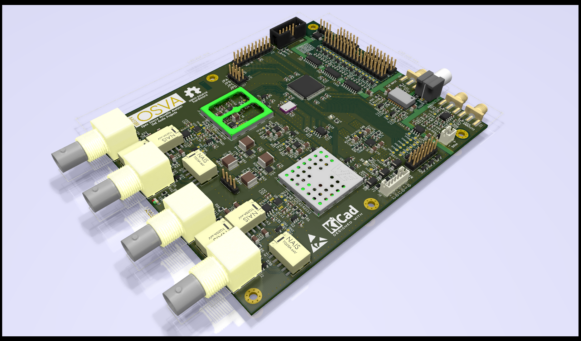
Thanks to Kicad, you can also see how it will look like when populated. 🙂
Now, i must order some missing parts to Mouser (a complete bom ready) to ready when i receive the board.
There is some works to be done on others PCBs of the project:
- Front panel control board (leds and rotary encoder)
- AAPSU Power supply board (+5 and +/-Vanalog).
- AA10M08 Digital Logic board (Digital filtering and display interface).
I must also seriously work on CPLD software.
I hope to give others new soon. To be continued...
Regards.
Frex
First, for the first release of the OSVA project, i start this new clean thread to avoid confusion.
This first post will be used in future to see major projects changes.
The OSVA is an new high performance analyzer that use SAR ADC from Linear-Technology/AD (LTC2380-24).
This project is born to follow up of my previous works done with the LT eval board and an CPLD eval board.
All information about this can be found on this previous post here :
SAR ADC for high performance audio ADC project [LTC2380-24]
So now, after some time of silence i keep you informed about project progress.
That has took more time than expected, time to learn Kicad too (and now Altium at work, Yuck!).
I do that only in spare time an i'm very busy at work right now).
Anyway, i now have finalized the PCB routing and i have ordered it to manufacturer (WEdirekt).
It will be on my desk, ready to start soldering in about ten days now.
From the previous schematics posted, i made several improvements.
I try to list them here :
Low noise regulators for ADC are replaced by LT3042 (as suggested by...).
- I added 2 isolated analog output from PWM signals for external oscillator synchronization (enable coherent FFT).
- The Input buffer LPF include two cutoff frequencies : 38.4kHz and 384kHz by default (they can be customized if required).
- The inputs can be switched to single-ended or differential mode.
- The input buffer is designed to use (at least) one this three buffers :
OPA1632 (SOIC8 FDA from Ti, lw noise).
THS4541 (High speed ultra low THD from Ti).
I planed at first time to use the ADA4945 that promised extremely low THD level, but the latest datasheet release
show much worse THD level so i will use preferentially the THH4541.
As this project is fully open source, you can get all project files in it's new GitHub repo here :
OSVA - Open Source Versatile Analyzer
Complete new schematic can be found here (pdf) :
Github AA2380v1.00 pdf file.
Thanks to Kicad, you can also see how it will look like when populated. 🙂
Now, i must order some missing parts to Mouser (a complete bom ready) to ready when i receive the board.
There is some works to be done on others PCBs of the project:
- Front panel control board (leds and rotary encoder)
- AAPSU Power supply board (+5 and +/-Vanalog).
- AA10M08 Digital Logic board (Digital filtering and display interface).
I must also seriously work on CPLD software.
I hope to give others new soon. To be continued...
Regards.
Frex

Cool!
To me it seems like the LT regs are better for LF and the TPS7A better for HF. You did it the other way, why? I may very well be wrong.
There is always Potato Semi. of you need faster flip-flop for that clock interface: Potato Semiconductor 74 Logic
After summer, right? Or?
Cost: 10, 100, 500, 1000, 5000€? Ballpark...
Good luck!!! 🙂
//
Hello,
LT3042 has better noise specs and above all much better PSSR, that is important to decouple from other noise sources.
It is also more expensive.
For the overall price, i have made a full bom file with Mouser/Digikey reference and that give a total cost of 296€.
This bom is available on the Github repo here.
About the final availability i really can't give you a date, sorry. That depends on personal events
and on time i will have. Anyway, it is on the right way 🙂
Did you have read my post ?
I just have send the Gerbers file to PCB manufacturer.
So, we will need to be patient before some measurements reports will be available.
I'm also impatient to start measuring with this !
Anyway if not know, you can show many measurements i made on the previous thread with the LT EVM (see here).
Regards
Frex
To me it seems like the LT regs are better for LF and the TPS7A better for HF. You did it the other way, why? I may very well be wrong.
LT3042 has better noise specs and above all much better PSSR, that is important to decouple from other noise sources.
It is also more expensive.
For the overall price, i have made a full bom file with Mouser/Digikey reference and that give a total cost of 296€.
This bom is available on the Github repo here.
About the final availability i really can't give you a date, sorry. That depends on personal events
and on time i will have. Anyway, it is on the right way 🙂
Are there already measurements or is this still all in progress?
Did you have read my post ?
I just have send the Gerbers file to PCB manufacturer.
So, we will need to be patient before some measurements reports will be available.
I'm also impatient to start measuring with this !
Anyway if not know, you can show many measurements i made on the previous thread with the LT EVM (see here).
Regards
Frex
Now, I'm quite certain I would not be able to assemble this myself. Will you somehow offer a working unit?
//
//
Are there any objections to skip the NB3N511 clock multiplier for the external clock and just apply an external clock signal of the desired frequency?
The 25 ps jitter of the NB3N511 are quite bad compared to the internal clock (80fs) or a decent external clock.
The 25 ps jitter of the NB3N511 are quite bad compared to the internal clock (80fs) or a decent external clock.
First, for the first release of the OSVA project, i start this new clean thread to avoid confusion.
This first post will be used in future to see major projects changes.
The OSVA is an new high performance analyzer that use...
This somehow sounds like a VERY interesting project. As I am totally new to your work, I may be totally in the wrong boat, but... how does this analyser interface to the software? Does it have a USB audio device interface? This would allow using it with the vast number of analysis software out there.
Hello,
I don't think.
Anyway, if there is some demand i would be possible to provide a fully populated board,
fully testes or not. But for now if it is a little bit early.
No problem.
You can use an external clock with the on-board 100MHz clock that is required to read data at high speed.
The external clock can be used only to perform CNV (conversion start) synchronization
Thank you.🙂
The OSVA is designed to provide for now at least a direct SPDIF output or USB interface
by using SDR-Widget I2S bridge (24/192k max) or Mini-DSP USB-Streamer that support
4x sliced I2S input to reach 24b/768k.
This is the first step of the project, but if i found some help it would be possible to send the full audio bandwidth
( 2x 24bits/1536kHz) using a Raspberry PI or FPGA board..
Frex
Will you somehow offer a working unit?
I don't think.
Anyway, if there is some demand i would be possible to provide a fully populated board,
fully testes or not. But for now if it is a little bit early.
Are there any objections to skip the NB3N511 clock multiplier for the external clock
and just apply an external clock signal of the desired frequency?
The 25 ps jitter of the NB3N511 are quite bad compared to the internal clock (80fs)
or a decent external clock.
No problem.
You can use an external clock with the on-board 100MHz clock that is required to read data at high speed.
The external clock can be used only to perform CNV (conversion start) synchronization
This somehow sounds like a VERY interesting project. As I am totally new to your work,
I may be totally in the wrong boat, but... how does this analyzer interface to the software?
Does it have a USB audio device interface? This would allow using it with the vast number of analysis software out there.
Thank you.🙂
The OSVA is designed to provide for now at least a direct SPDIF output or USB interface
by using SDR-Widget I2S bridge (24/192k max) or Mini-DSP USB-Streamer that support
4x sliced I2S input to reach 24b/768k.
This is the first step of the project, but if i found some help it would be possible to send the full audio bandwidth
( 2x 24bits/1536kHz) using a Raspberry PI or FPGA board..
Frex
1536kHz would be my preferred SR. 😀
And keep in mind that you may do the same failure as the RTX.
1. Building all in one PCB
. An Input over voltage would kill some simple parts and finally a full PCB with input & ADC & digital parts needs to be replaced.
. RF every were given form digital and ADC.
. To solve this requires a very high layered PCB what counts on the final cost.
2. My suggestion:
. Input attenuation (several steps) should be also separated and boxed and would be custom.
. Input amplifier should be boxed in a copper box. The benefit if this is blown, your separated input amp part still on live.
. ADC should be driven channel wise and driven from a proper oscillator as using Type SC-A sub-connecter.
3. Ground loops
. be careful with your tests where a star ground for proper measurements (as avoid hum)
. while a simple USB connections do some RF current flow trough the DUT even all running the DUT on battery ... source and sink of RF 😀
while running on HF, things gets worst even thinking all has been block by good ceramic cap's.
may look here about Grounding suggestions Audio Component Grounding and Interconnection
Hp
Hello all,
Some news today.
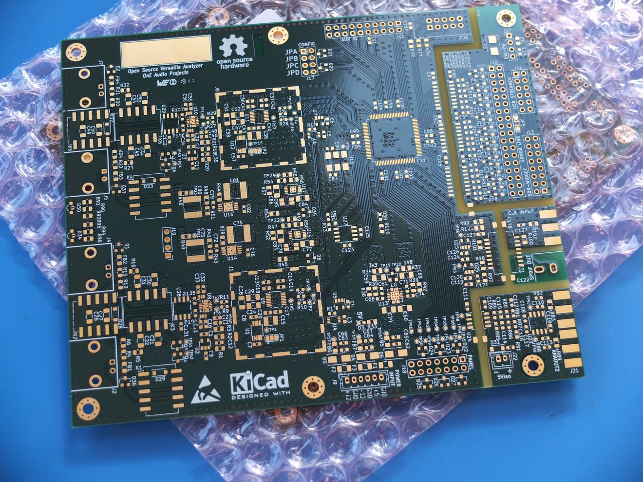
I received the AA2380 PCBs from WEdirekt and they looks good.
I must now finish to order some missing parts and the time to start soldering all of this...
A small picture speak more a long discuss:
I received today also my new hot air SMD working station (Quick861).
It will be used for small pitches parts soldering.
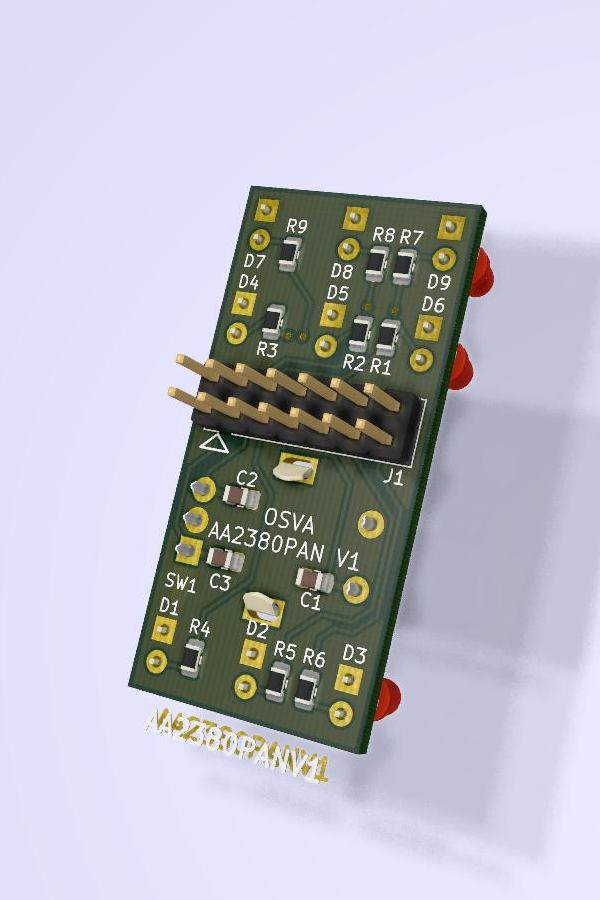
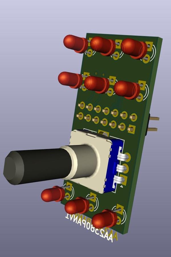
I have also almost finished the small PCB interface with the rotary encoder
and the panel leds. I will order this PCB in the week (i will try JLCPCB this time).
Just for fun, below a quick 3D rending of this PCB made with Kicad.
To follow...
Frex
Some news today.
I received the AA2380 PCBs from WEdirekt and they looks good.
I must now finish to order some missing parts and the time to start soldering all of this...
A small picture speak more a long discuss:
I received today also my new hot air SMD working station (Quick861).
It will be used for small pitches parts soldering.
I have also almost finished the small PCB interface with the rotary encoder
and the panel leds. I will order this PCB in the week (i will try JLCPCB this time).
Just for fun, below a quick 3D rending of this PCB made with Kicad.
To follow...
Frex
How much did you pay for the pcb?
And used layers 🙂
Hello,
I paid almost 200€ for 2 PCB.
It's not the cheapest, but they work fast and job is top quality.
I usually use PCBcart, but for 1-2 boars WEdirekt is well priced.
It's a class 5 four layers PCB (1 full ground internal layer, and one power rails internal layer).
Note that all files (including Gerbers) are available on the Github repo.
Frex
Hello,
Some project progress news today.
I just finished today SMD soldering of the AA2380 pcb, phew !
This is the first time i used a hot air gun and solder paste disposing.
Some tiny SMD packages with thermal pads are very difficult to solder otherwise.
I must say that it's a little tricky, but it went very well.
You can look below a picture of this partial result (only SMD for now).
Note that i don't have cleaned it yet, to tired for today ! 🙂
I had started to solder all SMD voltage regulators (critical tiny packages),
and after a first power-up after all output voltages are fine.
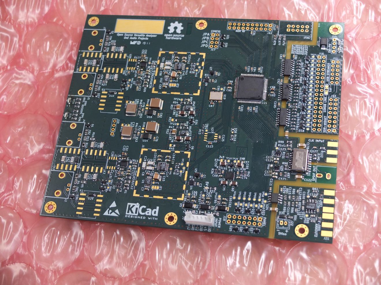
Frex
Some project progress news today.
I just finished today SMD soldering of the AA2380 pcb, phew !
This is the first time i used a hot air gun and solder paste disposing.
Some tiny SMD packages with thermal pads are very difficult to solder otherwise.
I must say that it's a little tricky, but it went very well.
You can look below a picture of this partial result (only SMD for now).
Note that i don't have cleaned it yet, to tired for today ! 🙂
I had started to solder all SMD voltage regulators (critical tiny packages),
and after a first power-up after all output voltages are fine.
Frex

- Home
- Design & Build
- Equipment & Tools
- OSVA - Open source Versatile Analyzer