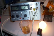
It is an E-variac + E-light-bulb combo:
I felt the need for such an accessory, because physical variacs cannot be electronically controlled (OK, they can be motorized, but it's not quite the same), and because incandescent light bulbs become rare, and are only available for a limited number of ratings.
This contraption emulates a variac, but it is combined with an original current limiter: the servo time constants (attempt) to emulate an incandescent light bulb: the capability to provide a large inrush current for a short period, and a constant current characteristic afterwards.
A big advantage over real light bulbs is the possibility of continuously tuning the emulated bulb power between 0 and 2500W.
The E-variac provides a maximum permanent power of 1500VA, and withstands short-term peaks of up to 25A.
It is unusual, in that it not based upon the classical AC supply scheme of Rectifier-PFC-Filter-Full bridge topology with its attendant bulk and complication.
A downside of this scheme is the inability to provide a voltage boost without topology switching, which is unpractical, but the upside is the full bidirectional capability: if a lower voltage is fed to the output, it is converted to a higher AC output at the input.
Not practical as an isolated feature, but very useful on reactive or power-generating loads.
The waveform shape is completely conserved: neither improved or degraded, a perfect image of the input.
Attachments
I use an old amplifier case with a 2 amp +/-45VDC supply.
If I power up an amplifier and if the transformer hums I know there is a short so I can quickly turn it off.
The 2 amps is low enough for most output transistors to survive.
For SMPS design I do use a variac in conjunction with a current detect circuit in the SMPS.
I turn up the variac slowly while monitoring current draw on my scope.
If there is enough interest, I'll try to provide usable information.
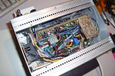
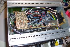
At the moment, the schematics are a bit like the innards: a serious mess.
The project started 2 or 3 years ago, and underwent mishaps, partial redesigns, and numerous modifications added layer after layer.
Ideally, I should have restarted from scratch at least one or two times, but I was reluctant to waste the work I had already invested, and I ended up with something that is working, but sub-optimal in a number of ways.
It is the version 1.245 of the initial project, but sensibly it should have been V3.2.2 or thereabout.
Duplicating such a monster without rationalization or streamlining would make little sense.
Attachments
OK, I will gather the bits and pieces. It will be some work, but it will be useful, even to me: I'll end up with some coherent documentation for my archives.
It may take some time though
It may take some time though
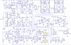
Here are the schematics: they will need some explaining, as they aren't exactly models of clarity.
I made them mostly simmable, which is good, but unfortunately it also increases the apparent visual confusion.
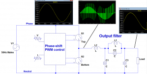
Here is already a quick description of the power topology (see first diagram).
The topology bears some resemblance with very particular cases of class D amplifiers, or cycloconverters, but the most accurate description is probably this one: it is a four-quadrant-in, four-quadrant-out, synchronous buck converter; at least it used here as a buck, but the multi-quadrant capability means that it can also operate as a boost.
The mains waveform is directly PWM-modulated by the power switches, without prior rectification or filtering.
This allows extreme simplifications compared to more classical schemes, but it also brings serious difficulties, the main one being the necessity for the switches to handle AC signals.
I made them mostly simmable, which is good, but unfortunately it also increases the apparent visual confusion.
Here is already a quick description of the power topology (see first diagram).
The topology bears some resemblance with very particular cases of class D amplifiers, or cycloconverters, but the most accurate description is probably this one: it is a four-quadrant-in, four-quadrant-out, synchronous buck converter; at least it used here as a buck, but the multi-quadrant capability means that it can also operate as a boost.
The mains waveform is directly PWM-modulated by the power switches, without prior rectification or filtering.
This allows extreme simplifications compared to more classical schemes, but it also brings serious difficulties, the main one being the necessity for the switches to handle AC signals.
Attachments
First, let's have a deeper look at the power section: I mentioned the difficulty of dealing with AC currents/voltages.
In fact, AC in itself is not particularly problematic: tested and proven solutions do exist. A diode bridge around the power elements is one, another is to use to anti-series MOSFets. Both work perfectly satisfactorily, and have been actually tested.
The diode bridge came up marginally better, which is why I retained it, but the antiseries works almost equally well.
The real problems are consequences of the AC operation: with a DC-operating half-bridge, you normally include dead-times to avoid simultaneous conduction, and use diodes to divert the flyback voltage to the supply rails.
That's perfectly OK for DC, but AC diodes do not exist (or they need to be synthesized with complicated circuits).
This means that you are not allowed to include dead-times; if they are present, they are the result of circuit inaccuracies and have to be dealt with.
Since there is no simple way to recuperate the energy, it has to be dissipated: the output filter is heavily inductive, and taming dead-time overvoltages means dissipating them in some kind of snubber.
This is a highly wasteful process: for this example (1.5kVA,20kHz), a 1µs dead-time represents 1/25th of half a period. The snubber would need to dissipate 1/25th of 1.5kVA: 60W.
Such a power was normal in the tube era, but for an energy-effective E-Variac, this is not tolerable: the dead-times need to be much, much smaller than this.
Conversely, simultaneous conduction is as (in fact even more) harmful: it results in destructive shoot-through current spikes.
How to navigate between those two Charybdis and Scylla?
That's what we will examine in the next post
In general, conventional (DC) power bridges rely on dead-times for safe operation: since the output node node can be left floating for few hundreds ns without major inconvenient, it is the simplest and safest solution.
The minuscule loss in duty cycle is normally negligible.
With AC circuits, adopting the same technique would be possible, but wasteful: because safety margins are required to cope with dispersions, temperature variations, etc., the dead times need to be significantly larger than the theoretical minimum possible, leading to high losses in the snubbers or voltage transients absorbers.
Here, the timing of the drive signals has been made as accurate as possible, and the inevitable residual errors are dealt with with two types of snubbers: transient suppressors for overvoltages, and inductive snubbers for cross-conduction.
Bidirectional Transils handle overvoltages in a pretty standard way, but the inductive part is somewhat smarter:
The inductors are coupled, and inserted in the DC part of the circuit (the drains of the MOSfets)
Because they are coupled, they behave like a single virtual inductor which doesn't see the 20KHz switching. This is important, because separate inductors would store and release energy for each switching half-cycle, leading to significant losses: at 7A, 5.7µH inductors store 140µJ, which amounts to 2.8W at 20KHz.
Another advantage of the coupled inductors is that the inductance available to absorb cross-conduction pulses is 4 times the value of each individual inductor, compared to 2 for separate ones.
Thanks to the DC operation, the energy generated by the shoot-through pulses can be eliminated simply, using a conventional diode+resistor scheme.
This is one of the advantages of the rectifier bridge over the anti-series MOSfet connection: the DC is explicitly present.
A word about the diode bridges: At first sight, it would seem that standard, slow-recovery diodes would suffice: the diodes do carry the 20KHz signal, but they only switch at 50Hz.
On the first versions, I had indeed used slow diodes, but under very particular conditions, anomalies became apparent.
I first realized that in fact, the diodes could also switch at 20KHz for peculiar combinations of load and duty-cycle, because the reactive nature of the output filter could force a current inversion mid-cycle.
But that in itself wasn't sufficient to cause problems: even when the diode pair was in recovery mode, the corresponding MOSfet was still able to put the power module out of conduction.
The actual problem was more subtle than that: it appeared only when a 20KHz switching event happened just after the reactance-induced current inversion: at that moment, all 4 diodes of the module were in recovery mode, causing a dead short, with no control possible from the MOSfet.
This generated huge shoot-through events that overwhelmed the inductive snubbers.
The problem was particularly nasty, because it only manifested itself under a very narrow range of conditions.
In the end, I figured out what was going on, used fast diodes (BY229) and the problem was solved.
The output filtering is carried out by L3/C11, with a notch filter centered at 20KHz perfecting the job (because of the various servo loops, the main filter components cannot be too large).
Note that C11 cannot be an X-type capacitor: these capacitors have a shallow metallization, and do not withstand any permanent ripple current.
Here are the schematics: they will need some explaining, as they aren't exactly models of clarity.
I made them mostly simmable, which is good, but unfortunately it also increases the apparent visual confusion.
Here is already a quick description of the power topology (see first diagram).
The topology bears some resemblance with very particular cases of class D amplifiers, or cycloconverters, but the most accurate description is probably this one: it is a four-quadrant-in, four-quadrant-out, synchronous buck converter; at least it used here as a buck, but the multi-quadrant capability means that it can also operate as a boost.
The mains waveform is directly PWM-modulated by the power switches, without prior rectification or filtering.
This allows extreme simplifications compared to more classical schemes, but it also brings serious difficulties, the main one being the necessity for the switches to handle AC signals.
Thanks Elvee for sharing this. Please note that CD4030B, CD4013B and LM393 models are missing.
The CD4000 ICs come from a library downloadable on the Yahoo group:
https://groups.yahoo.com/neo/groups/LTspice/files/ Lib/Digital CD4000/
(CD4000.lib)
I also found the LM393 model there.
Here is the symbol LM393.ASY:
Version 4
SymbolType CELL
LINE Normal -32 32 32 64
LINE Normal -32 96 32 64
LINE Normal -32 32 -32 96
LINE Normal -28 48 -20 48
LINE Normal -28 80 -20 80
LINE Normal -24 84 -24 76
LINE Normal 0 32 0 48
LINE Normal 0 96 0 80
LINE Normal 4 44 12 44
LINE Normal 8 40 8 48
LINE Normal 4 84 12 84
WINDOW 0 25 32 Left 0
WINDOW 38 25 96 Left 0
SYMATTR Value LM193
SYMATTR Prefix X
SYMATTR SpiceModel lm193.sub
SYMATTR Value2 LM193
SYMATTR Description Universal Subcircuit for OpAamps from ST(SGS-Thompson)
PIN -32 48 NONE 0
PINATTR PinName In-
PINATTR SpiceOrder 1
PIN 32 64 NONE 0
PINATTR PinName OUT
PINATTR SpiceOrder 2
PIN -32 80 NONE 0
PINATTR PinName In+
PINATTR SpiceOrder 3
PIN 0 32 NONE 0
PINATTR PinName V+
PINATTR SpiceOrder 4
And here is the model:
* WARNING : please consider following remarks before usage
*
* 1) All models are a tradeoff between accuracy and complexity (ie. simulation
* time).
* 2) Macromodels are not a substitute to breadboarding, they rather confirm the
* validity of a design approach and help to select surrounding component values.
*
* 3) A macromodel emulates the NOMINAL performance of a TYPICAL device within
* SPECIFIED OPERATING CONDITIONS (ie. temperature, supply voltage, etc.).
* Thus the macromodel is often not as exhaustive as the datasheet, its goal
* is to illustrate the main parameters of the product.
*
* 4) Data issued from macromodels used outside of its specified conditions
* (Vcc, Temperature, etc) or even worse: outside of the device operating
* conditions (Vcc, Vicm, etc) are not reliable in any way.
** Standard Linear Ics Macromodels, 1993.
** CONNECTIONS :
* 1 INVERTING INPUT
* 2 NON-INVERTING INPUT
* 3 OUTPUT
* 4 POSITIVE POWER SUPPLY
* 5 NEGATIVE POWER SUPPLY
*.SUBCKT LM193 1 3 2 4 5 (analog)
.SUBCKT LM193 1 3 2 4 5
.MODEL MDTH D IS=1E-11 KF=1.050321E-32 CJO=10F
* INPUT STAGE
CIP 2 5 1.000000E-12
CIN 1 5 1.000000E-12
EIP 102 0 2 0 1
VIO 10 102 438.3U
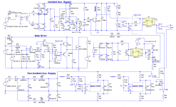
PWM, Phase-shift & drivers
The master oscillator is U1B; it feeds the sawtooth generator U1D.
This 40KHz sawtooth serves as a reference for the PWM modulator, U1C.
The 40KHz PWM signal is converted into a 20KHz phase-shift modulation by the two flip-flops U2A and B. On their output, a 20KHz squarewave having an exact 0.5 duty cycle is always present.
The rest of the circuit (U1A and passives) "parks" the modulation at the limits and allows duty-cycles of very nearly 0% to 100% without risking the loss of one of the signal, which would be catastrophic.
Why the complication of this phase-shift modulation?
It allows the transfer of an information including DC (0% or 100%) with a few ns accuracy and resolution, using only two gate transformers for two power devices, without auxiliary gate supply and never subjecting the gate transformers to duty-cycles different from 0.5.
That's a whole lot of advantages in one swoop.
That said, I have now found even better options, but I didn't want to redesign the whole thing and didn't incorporate them in my final prototype; it is working well enough.
The flip-flops drive the gate transformers via transistor H-bridges. Each transformer has two secondaries, and each gate receives its drive through a circuit combining two secondaries in coincidence or anti-coincidence, to decode the phase-shift information.
The main schematic shows the early version of this decoder using discrete transistors. In the final circuit (see other schematic), I have adopted a different circuit, based on XOR gates, because it allows a very accurate fine-tuning of the timing, which is crucial for this topology.
I kept the early version on the main schematic because it simulates more easily.
Note that some components non-essential for the simulation have been omitted: supply bypasses and isolation circuits, common-mode chokes on every signal to the gates etc.
In addition, the construction of the gate transformers is highly critical.
Also, all the circuits share a common ground, because it is necessary for the sim, but it is obvious that in reality the drive circuit is isolated from the mains.
I also remind that I advise strongly against attempting to build the circuit as it is shown, it should only be used a source of inspiration for people competent enough to brew their own version.
If I had to build a second prototype, it would be quite different from this one.
Voltage control loop
This instrument can work as a "dumb", ordinary variac by directly acting on the PWM ratio, but it also has a provision for servoing the output voltage.
Both the voltage and current loops present difficult challenges: unlike a class D amplifier-based AC supply, where the loops operate in "real time" at the switching frequency, this variac uses leveling loops or AGC's acting on the 50Hz output.
This seriously limits the possible speed of the servo: the magnitude of the voltage first needs to be acquired by rectification and then filtered.
Unfortunately, a too sluggish regulation is not very useful: for the voltage, it could compensate for slow variations only, and for the current, it could lead to dangerous overshoots.
In principle, there is a tradeoff between the quality of the filtering and the speed.
Ideally both are necessary: if too much ripple remains, the output waveform will be modulated and distorted, and if too much delay is introduced, this will impose a slow response to keep the loop stable.
Here, an unusual strategy has been used to eliminate the delay and ripple caused by filtering.
Since the phase and frequency of the output signal are known, because they are locked to the input, it is possible to use that additional information to construct a minimum-delay, zero-ripple acquisition front-end.
U5D plays the role of the full-wave precision rectifier, but it is not followed by a conventional LP filter: instead the output is sampled at the waveform peaks by a switching transistor, and held for the rest of the time.
That way, the maximum delay is 10ms, and there is no ripple.
U3A and B are a window comparator creating the sampling pulses from a quadrature waveform derived from the input.
The rest of the circuit is a conventional regulator built around U5B, transmitting its output through an optocoupler to the PWM modulator.
Current control loop
The current loop cannot use the same trick as the voltage one, because the phase relationship between the output voltage and current is unknown, but fortunately its requirements are very different:
Since it is supposed to emulate a light bulb, it is made deliberately slow -mostly-
one part that cannot be slow is the protection of the variac itself.
For these reasons, the regulation loop is of the PI variety, with a very dominant and long time-constant integral component, and a unity-gain proportional component.
U4A & B form the precision rectifier receiving its input from the current shunt R48 and also a fraction of voltage-derivative injected by C18/R55.
This addition is required to keep the loop stable.
The regulator is U4D: it compares the measured current to the value set by the current pot; C16/R53 establish the time constant.
The output of the regulator feeds an optocoupler controlling the PWM modulator, and also drives a LED via Q16 when the current loop is active.
The proportional part of the loop makes it very fast in case of a severe overcurrent, like a dead short for example. The worst case peak current in the MOSFets remains below 35A, for only a few microseconds.
It is normally safe, but I have also included a fast overcurrent trip, independent of the regulator (see second folio of the schematic): when an unexpected and brutal short occurs, it is preferable to halt things completely.
The voltage across the shunt (named R20 here) is rectified by a diode bridge and feeds the LED of another optocoupler linked to a small SCR.
This SCR activates the power-ON-reset transistor Q1. The resetting is achieved by shorting the SCR, making the reset impossible in case of a persistent fault.
- Status
- Not open for further replies.
- Home
- Design & Build
- Equipment & Tools
- Here is my new E-baby: