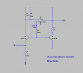
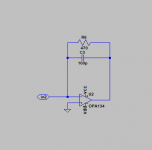
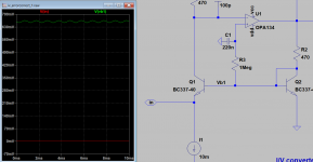
Today looking at a circuit that a forum member posted I had an idea to build an I / V converter that uses error correction to lower the input impedance, the circuit is interesting because the input transistor Q1 although not in the feedback loop of the op- amp has low distortion and low input impedance, the collector is connected to the negative pin of the op-amp, there is no variation of voltage in Vce of this transistor, so there will be no distortion due to early effect.
R3 and C1 are used so that the currents in Q1 and Q2 are exactly the same, which allows maximizing the effect of the input error correction.
Q1 and Q2 preferably should be a double transistor.
C2 will compensate the error correction loop.
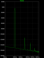
First photo is the circuit , second the input impedance, third is distortion with 4mA p-p @ 1kohm impedance
R3 and C1 are used so that the currents in Q1 and Q2 are exactly the same, which allows maximizing the effect of the input error correction.
Q1 and Q2 preferably should be a double transistor.
C2 will compensate the error correction loop.
First photo is the circuit , second the input impedance, third is distortion with 4mA p-p @ 1kohm impedance
Attachments
Cool idea. What limits the effectiveness of this error correction is the fact that I(R2) does not exactly match I(R1), because of the nonlinear Vbe of Q2. Also, the Vce of Q1 and Q2 don't match, which could conceivably introduce some error.
What issues specifically is this circuit intended to solve?
What issues specifically is this circuit intended to solve?
Take a better look at the circuit Kean, Vce of Q1 and Q2 are the same.
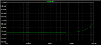
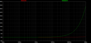
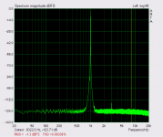
The input impedance with the error correction will be lower and more linear that the classical opamp iv converter, in the second image we can see the input impedance of the classical circuit in green and the error correction circuit in red,
both circuits use OPA134.
Note that I only had this idea a few hours ago, I did not have much time to optimize the circuit.
Attachments
Yep, I noticed that after I posted.
I wonder why you chose not to use a logarithmic scale... Orange is your circuit input impedance, red is the vanilla LT1028 input impedance. The lower orange trace is with R2 trimmed. The input impedance of this circuit is highly dependent on transistor matching. R2 can be used as an impedance trim with no penalty for distortion assuming the transistors are matched well enough to fall within a reasonable range (I think they will be matched well enough from the factory to be trimmed).
This brings up another problem. The optimal trim value for input impedance will probably not be the same value for 0V offset. What then?
Lots of little things to bite at your ankles... 😀
Attachments
Last edited:
That depends on how much tolerance you put on the word "same".smms73 said:Vce of Q1 and Q2 are the same.
For DC conditions Vc will be the same, apart from opamp offsets. Ve of Q1 is undefined, so we cannot say that Vce is the same for both.
For AC Vc1 must vary in order to get a signal through the circuit.
Why do you want Vce to be the 'same' anyway?
The error caused by the delta Vce depends on the voltage gain limit of the transistors used. For good transistors it is over 70db, but can go as low as maybe 45db, and then lower if the transistor is in quasi-saturation.
Likewise, the voltage at the opamp input will be mitigated by the input transistor's voltage gain limit, I think it will be practically insignificant, as far as causing error at the input, although the opamp error still shows up at the output.
However I don't think this circuit does much to reduce the distortion created by the opamp itself. The premise is that a lower input impedance will mean less distortion coming from the DAC. I don't know the details about that or the significance of the effect, but I do know that generic opamp IV converters seem to do fine in measurements if you use a good opamp. So really the struggle here is to keep the discretes from generating any significant amount of distortion. And of course the discrete input can have lower noise.
Last edited:
The premise is that a lower input impedance will mean less distortion coming from the DAC. I don't know the details about that or the significance of the effect, but I do know that generic opamp IV converters seem to do fine in measurements if you use a good opamp.
Depending on the DAC used, with the pcm1794 an impedance of 50 ohms is low enough to only produce 0.0005% distortion.
6 years ago I also measured the distortion of the es9018 depending on the input impedance (and I ended up destroying a rather expensive Dac in the process), these measurements were made with four channels in parallel.
With 195 ohms the difference in distortion is notorious, but between 10 ohms and zero it is completely irrelevant
first photo with 195 ohms of impedance, second photo with 10 ohms and third with zero.
Attachments
That depends on how much tolerance you put on the word "same".
For DC conditions Vc will be the same, apart from opamp offsets. Ve of Q1 is undefined, so we cannot say that Vce is the same for both.
For AC Vc1 must vary in order to get a signal through the circuit.
Why do you want Vce to be the 'same' anyway?
Agree. This is not an optimum way to do it, it will drive the Vce of the input Q towards zero. Why would that be a Good Thing?
More effective imho would be to use the servo to keep the input emitter at zero volts.
Jan
please Jan take a better look at the circuit,
Yesterday I have build this circuit in a breadboard, the voltage in Q1 collector is 0.636V the emitter voltage is 500uV , the voltage at Q2 is 0,636V
0.636V of VCE is enough for the bc337 as VCEsat are very low in this type of BJT
Yesterday I have build this circuit in a breadboard, the voltage in Q1 collector is 0.636V the emitter voltage is 500uV , the voltage at Q2 is 0,636V
0.636V of VCE is enough for the bc337 as VCEsat are very low in this type of BJT
The measured input impedance was very low , with 0,5 ohms at 1MHz and 10 ohms at 10Mhz, the impedance was much lower at 100khz, impossible for me to measure with my oscilloscope
please Jan take a better look at the circuit,
Yesterday I have build this circuit in a breadboard, the voltage in Q1 collector is 0.636V the emitter voltage is 500uV , the voltage at Q2 is 0,636V
0.636V of VCE is enough for the bc337 as VCEsat are very low in this type of BJT
I understand. I was just wondering why doing this would be a Good Thing?
You are not really interested in Vce, are you? You are interested in Zin. I don't see the connection.
Jan
As This circuit uses Q2 to correct the errors in Q1, is important that current and voltage are "almost" the same
I don't think so. Q2 doesn't correct anything, it sets the bias for Q1. The additional circuit makes the Vce of both about 0.6V as you said. I cannot see any advantage in that, can you explain to me please? What is your rationale to make the Vce so low, even using an opamp specifically for that?
Edit: Looking again at the circuit, the transistors should, at a first order, have the same Vbe and thus the same collector currents, right? Since they also have the same collector resistor, they will also have the same Vce. Without any additional circuit.
Jan
Edit: Looking again at the circuit, the transistors should, at a first order, have the same Vbe and thus the same collector currents, right? Since they also have the same collector resistor, they will also have the same Vce. Without any additional circuit.
Jan
Last edited:
Exactly, and since Ic in Q1 is always equal to Ic Q2, Vbe2 is also always equal to Vbe1, so the variation of Vbe in transistor 2 will serve to override the voltage variation in the emitter of Q1 (in).
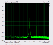
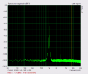
In this picture is the voltage variation at the base of Q1 (green) and the voltage at the emitter at Q1 (red) when a signal of 4mA p-p of 1khz is connected to the input.
as the variation in (IN) is 85uV p-p the impedance at 1khZ is only 0.02ohms
Also the ltspice file if someone want to test by themselves
Attachments
Although i do understand the importance of the input impedance to be low, i think it's counterproductive if you have it THAT low outside the audio band .
For that i took a small step forward including the low pass passive filter inside the loop giving me the option of using very low noise and ultra low distortion "audio" op-amps which usually have less slew rate than needed for the i/v job.I bet i can do it with opa2227 at 2.3v/us.After my epic fail with ada4898-1 melting down, and being disappointed by the higher noise of lm6172 for lower output dac's of the past , i simply thought of going back to my first idea and it seems that failure is the mother of all good things 🙂
New i/v stage in town
I will build it this days the same as i did with my first version, but I'm absolutely sure that it will work wonderfully after i found the real needed values for that filter.As i'm not a true engineer(unfortunately very few engineers really helped me in life), I'll do it through the same process of trial and error that always helped me.
Last edited:
I've seen literally nobody on Diyaudio asking how and why some of the best Denon and Nakamichi cd players of the past used upc4570 as i/v and ne5532 just for buffering although the first has a 3x lower slew rate...And you have that in some players that used copper all throughout ,very expensive parts and laser and even two different transformers, one for analog and one for digital supply...Some other weird , but reputable players used m5220 as i/v and again ne5532 as output buffer and low pass filter...how come?
I think I've read again and again all sort of topics about the best op-amp in I/V conversion and none of them mentioned this aspect or even worried about...or tried to explain that .Or maybe i just skipped the class...🙂
I think I've read again and again all sort of topics about the best op-amp in I/V conversion and none of them mentioned this aspect or even worried about...or tried to explain that .Or maybe i just skipped the class...🙂
- Status
- Not open for further replies.
- Home
- Source & Line
- Digital Source
- Simple I/V converter with error correction