Hi All,
I have an old Theta DSPro Gen II DAC. Its from the days of SPDIF input only, which is becoming quit the anachronism. At minimum i would like to add USB input; ideally I'd add an Ethernet input (maybe a Pi).
While i could spit out SPDIF, which it takes in, that seems silly - I2S would be a better interface, especially since i expect to do this within the case.
The problem is that there are no schematics, and worse, Theta went to significant trouble to obscure the chips that are in there. Does anyone have a schematic, detailed block/function diagram, or info on whether i can gain access to an I2S interface and if so where/how?
TIA,
G
Some info about the dac chips here: Theta DSPro Generation II DAC; D/A Converter - The Music Room
Some other info at: Attempting to fix Theta DS Pro Gen II | Super Best Audio Friends
Comment: What you want to do probably could be done, but seems doubtful its worth all the effort to reverse engineer the unit enough to modify it properly. There would of course be risk of damage too.
Therefore, my suggestion would be to get a good USB board that can output SPDIF and use that. A very good one with an exceptional feature set (ultra-low jitter clocks, galvanic isolation, etc.) is: I2SoverUSB - I2S over USB Audio
Last edited:
Thanks for the info Mark W4. The first page was just and ad, and the info was merely the Mot PGAs and the AD 1860 chip - all known.
But the 2nd was actually a treasure trove. If that is indeed the Word Select, Bit clock and L & R data it may well be possible to I/F I2S there..in fact that may be the stage immediately after I2S - once the WS has been executed.... need to ruminate on that one.
or as you say, move along and get a good USB - > SPDIF adapter (or better yet ethernet end point to SPDIF adapter).
The Schiit EITR, BTW, plays very badly with the DSPro. interesting since MM designed both.
Thanks again
G
Eventually i plan to dig in and design my own, but the study-ing necessary is in queue with more urgent things ")
So in the meantime I think one of these boards is a nice short-cut on an interesting museum piece that still sounds good, but not great by the best 2020 standards.
Do you have any experience or opinion on three options:
1. the one you mentioned
I2SoverUSB - I2S over USB Audio
2. Twisted Pear
The USB DAC/Receiver
3. DIY in HK
https://www.diyinhk.com/shop/audio-...tput_socket-yes/usb_socket-type_b_traditional
TIA!,
G
1. Great clocks, galvanic isolation, highly configurable, etc.
2. Nowhere near in the same league as #1.
3. This one has been known to blow the XMOS chip sometimes when plugged into a USB cable. Apparently there is no protection circuitry, as recommended by XMOS. No galvanic isolation, same clocks as #1, but a similar USB board by the same manufacturer and with the same clocks sounded inferior to #1. Lack of isolation may have been a factor, another factor could be some implementation problems with clock power, decoupling, ground plane currents running under the clocks, etc.
...However, #3 might be a good choice for someone wanting to try some diy reprogramming of the XMOS chip.
Last edited:
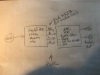
Thanks, plus high level blokc diagram and quick analysis of Theta
Thanks Mark,
Absent any direct "BTDT" on the others i picked up the board you suggested.
It ought to do the trick well.
More generally:
Theta DSPro Gen 2/input and functional blocks:
______________________________________
I did some digging on the layout of the DSPro, which is an adventure since there is no documentation.
As it turns out, gaining access to I2S is very difficult. In fact, it may be thoroughly impractical without eliminating much of what's good about the Theta.
From what i can figure out, the basic flow is per the sketch i made below (attached, figuring out this editor):
The issue is that the S/PDIF interface directly feeds the shift registers, memory and FPGAs that form the input and digital filters of the Theta. And i doubt any of us want to reverse-engineer he obscured parts and design of this 40 year old beast. The bit-word-data (L/R) interface exists only between the FPGAs/filtering (Mike's secret sauce) and the D/A chip. So out the baby would go with the bathwater if i decided to plug in at hat point. Although, for all you "non over sampling" fans, maybe that's an option.
It seems that the SPDIF is he best choice, and even more importantly, it appears that the digital circuitry completely re-clocks whatever goes in anyway (its going through FPGAs and memory after all) so what's the point?
Maybe someone will find this helpful.
G
Attachments
Thanks again.
For the record, i bought the USB over I2S board, installed it in the Theta. I powered the USB I/F from the USB cable, tapped off the +5 internally and built an isolating/filtering stage to power the reclock/etc., configured for S/PDIF (yiked, hand soldering SMD resistors - not fun), and made a nice shielded COAX to the S/PDIF input.
I kept the S/PDIF coax very short and well shielded.
I put a bit of effort into the power with C-L-C isolation and a lot of very local filtering. Note this is for only the isolated portion of the board - he noisy side is line powered.
Works great.
Note the Theta will not synch properly with algorithm #1.
Sonically, this is surprisingly good. VASTLY better than the Theta with either a CD player input or a Schiit EITR input. Vastly. In fact it shocked me - i just wanted a solid, convenient way to use a very interesting old DAC (one i kept mostly as a museum piece as I believe the Gen 1 (this is gen 2) was pretty much the first of its kind).
It is now doing some things sonically that my modern DACs are not.
I need to measure but i suspect the jitter is very low.
G
pictures are somewhat difficult only because the unit is in use, and somewhat buried. I'm happy o answer any questions or sketch a diagram. Its really pretty straightforward. I2S over USB board. Set to SPDIF configuration, and isolated USB power. More info from the supplier. Clean side powered by clean power. tapped the Theta's 5V analog power supply, created an LC filter to isolate this board. Took the SPDIF output and ran to the Theta's SPDIF input. mechanical mounting is pretty much wherever you find i fits. I2S over USB needs to poke out the back for USB. I put my LC on the power supply side and ran wires. No magic.
Unless you really desire to tinker inside the DAC for the fun of it, I suggest that you seriously reconsider your plan, and utilize an external USB-to-SPDIF converter, such as the HiFace, instead. Modifying the innards of your DAC comes with the risk of the modification not working for some reason, and also risks damaging the DAC beyond easy repair.
I realize that mounting all of the conversion circuit parts inside the DAC box is visually more elegant, but something like the HiFace unit is only minimally visible once the DAC is sitting on your equipment shelf. As far as the resulting net system jitter being lower via a direct I2S connection, that’s possible, but not automatically true. Even should your modifications fortunately result in less measured jitter, I shouldn’t be surprised if the difference were not audible.
Think carefully about the risks versus the reward. Just my two cents.
- Home
- Source & Line
- Digital Line Level
- Theta DS-Pro Gen 2 info