Taobao CPU on promotion
I've just ordered one of these STM32H750 boards as the price is a tad over $7.
???STM32H750VBT6??? ??QSPI?? CubeMX STM32H7???-???
This CPU is something of a beast in the world of M-series. It runs at 400 (or maybe even 480) MHz and is dual-issue, meaning some instructions can run in parallel. It even has a double-precision FPU. What's particularly unusual for an ARM SoC is it has an on-chip S/PDIF-AES/EBU receiver and also 4 channels of S/PDIF output. The reference manual is equally a monster, running to over 3300 pages.
Here's a jolly useful resource I have only just discovered : TFilter - Free online FIR filter design
A very convenient way to design FIR filters! More flexible and powerful than other free FIR design software I've downloaded in the past.
A very convenient way to design FIR filters! More flexible and powerful than other free FIR design software I've downloaded in the past.
STM G4 series eval board
Taobao now has these STM32G431 eval boards for under $7 : ??STM32G431CBT6??? STM32G4??? ??? ???-???
While 170MHz isn't the fastest available M4 CPU its enhanced here with a math accelerator 'FMAC' which could boost its effectiveness in implementing FIR filters so long as the data and coefficients aren't longer than 16bits. There's also a hardware random number generator which should come in handy in generating dither.
monoDAC prototype
Here is the first realization of an idea I've had brewing in my mind for some time - a mono DAC - i.e. just a single channel on a board. Which channel is decoded from the stereo pair is selectable with a switch as I2S sends both channels to each board. The other interesting aspect here is that its using an ARM MCU to fiddle the channels around on I2S. The filter isn't a separate board as on 'Deca DAC' rather its built-in as the intention is to have filters from now on in software rather than hardware. I've implemented a 5th order Chebyshev and eventually I'll get the MCU to do 2X OS but for now its running NOS.
The MCU daughter board on the monoDAC is a 'Blackpill' which is a cheap and cheerful Cortex M4 board using an STM32F401 (or optionally, an F411). The F401 runs at 84MHz and has a couple of full duplex I2S ports. Blackpills are available (hopefully, with the current supply squeeze on MCUs) on Aliexpress and eBay.
$3 STM32 "Black Pill" Board Features STM32F4 Cortex-M4 MCU, Optional SPI Flash - CNX Software
What's nice about the STM32F401 is its one of the lowest power M4s on the market, sipping about 140uA/MHz.
Attachments
Once I proved the concept - got the I2S peripherals running - the first real experiment was to slow down the I2S. This is something I've done in the past with logic, then at the start of this thread with the STM32F030 helped by external logic to adapt its SPI to I2S duty. This is my first time for doing that using native I2S peripherals. I figured it should be much easier.
But the problem with slowing down I2S is how to generate the new, half-speed clock. A flip-flop is an obvious first choice but it not only has to be divided by 2 from the input BCK it also needs to run in the correct phase. The FF can start up in one of two possible states - a prod into its reset pin driven by the MCU is one way to achieve phase synchronization but I was curious if there was any internal logic (internal to the MCU) which could obviate the need for the external FF with accompanying reset code.
At first I figured a timer might do the job and the F401 has plenty of those, though not all can accept an external clock input. The phase sync problem still remains though which calls for fiddly software. At last it dawned on me that I could use the spare transmit half of the I2S input (F401 supports full duplex I2S) to create the half speed clock. So now I'm using the Data output (outputting 0xAAAAAAAA in 32bit mode) of that port into the BCK pin of the output I2S and it seems to work fine.(*)
The Tx half of the input I2S could also in theory generate a phase-sync'd double-speed WS for when I implement the 2XOS code. With the input fs at 2.8MHz the 2XOS output port runs at the same as the input clock rate, just in 16bit mode.
(*) I feel I should point out that the CubeMX software can't quite manage the trick of the two halves of a full-duplex I2S peripheral running in different modes - 16bit on receive and 32bit on transmit. So I had to resort to assembler for that.
Last edited:
Very interesting !, could you elaborate about your goals and solution ?
I figure that input I2S adapter is slave (clocked by the transport) and output I2S adapter is slave to, but clocked by the output channel of the input I2S adapter continuously sending a 0xAA pattern, that’s the trick, well done !
What are I2S frames size of your input (from transport) and output (to TDAs) ?
Chris
My overall goal here is to adapt my DAC design to be easier to manufacture and hence cheaper. Smaller too if possible. The time-consuming part in the build process (I'm speaking about Dena DAC which is the latest incarnation of my designs here : lingDAC - cost effective RBCD multibit DAC design) is the 7th order LC filter which requires close-tolerance inductors and caps to get a relatively flat FR and well-defined cut-off behaviour. Using 2XOS I hope I can get away with a simpler 5th order filter with wider tolerance components.
But that's not the only goal here - I'm interested in trying out a few things and having a play to explore the limits of what these DAC chips can do. The half-speed I2S is one such avenue. Splitting up the 10 channels (I'm using 5 stereo chips) into two groups of 5 and sending slightly different signals to each is another interesting area which I plan to explore.
Your conjecture is correct - input is slave (16bits filled in 32bit field), output is also slave and fed by the synthesized 1.41MHz clock (16bits in 16bit field). Does this answer your question?
Thank you, I think I get it.
Your software DSP receive a stereo I2S stream, 44.1k, 16b/32b frame, pickup one channel, do some calculation and issue a two channels I2S stream 44.1k, 16b/16b frame in order to feed two DAC groups which outputs will be mixed to provide a single audio channel. Your DSP run NOS but can easily run 2xOS by having the output SPI adapter clocked by the input clock rather than the half.
If not secret or too early, what kind of treatment do you apply to the mono input signal of your DSP in order to produce two different I2S streams intended to be DA converted separately the mixed to together?
Chris
The kind of treatment I'm thinking of is adding +noise to one set of channels and -noise to the other set. So that, to a first order the noise cancels. The idea being to randomize the bit-weight errors at the LSB end of the DACs.
The F401 doesn't have a random noise generator in hardware so at first I plan to use the ADC to digitize an external noise source (TL431 from a lower-end manufacturer).
The F401 doesn't have a random noise generator in hardware so at first I plan to use the ADC to digitize an external noise source (TL431 from a lower-end manufacturer).
That looks like dithering, but I don’t know about the expected effect of the difference after D/A conversion.
That’s very interesting to have such a platform which allows practical assessment of signal processing theory. A very DIY initiative !
Thanks for publishing.
That’s very interesting to have such a platform which allows practical assessment of signal processing theory. A very DIY initiative !
Thanks for publishing.
@AIM65 - you're welcome 🙂
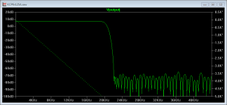
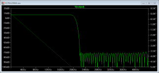
Before writing the code for the 2XOS filter I wanted to play with a few filter responses to see what kind of stop-band performance is possible and how it relates to the precision of the filter coefficients. The online calculator I linked in post #22 is an excellent resource but it only gives the filter response in almost perfect double precision. It gives out filter coefficients in integers but doesn't show the degree to which the response is degraded by reducing their bit length.
I decided to turn to Kendall Castor-Perry's method of simulating an FIR filter using LTSpice's delay line component. This gives rise to the results shown below - the first is the response of a typical 2XOS linear phase filter with 125 taps and 16bit precision. The second shows how the stop-band performance improves with 2 extra bits on the coeffs.
Attachments
If you use assembly I figure out it could be difficult to use Cortex M4 FPU and DSP.
But have you tried to use C and arm_math.h CMSIS library, it allows you to unleash DSP and FPU and to run float or double or Q calculations. I’ve no experience with it, but a lot of ideas and plans for experimentation…😀
With this library I figure you would be able to use 16bits sample as input, do 24 or 32bits calculations, then truncation, then dithering, then D/A with the TDA groups. On the other hand, it’s very likely that reaching as many tap numbers than in assembly will be hard.
Ref : Finite Impulse Response (FIR) Filters
Chris
About 10 years ago, before Cortex M4 was easily available I wrote FIR filters for both the M0 and M3 in assembler. So I already have code which shouldn't be too difficult to adapt to take advantage of the extra instructions onboard the M4. And I'm making some progress on this - understanding the M4 DSP extensions - so I'm fairly confident I'll have something working in the next week or so.
I haven't tried to use C on these ARM MCUs, no. I have had some experience of writing C but didn't much enjoy that. I have had more experience of turbo charging C programs using inline assembler to get improved DSP performance and that was a LOT of fun. That was in the days of MC68020 and MC68881 where the C compiler didn't have a clue how to get the best FP performance out of the processor-coprocessor combination.
I use assembler simply because I enjoy the process much more - C coding is too abstract and then even after coding there's the inevitable process of finding out how the compiler's too dumb to minimize the execution time. I have a useful benchmark in C - Paul Beckmann's AES paper on DSP is an excellent resource (I'll link to it at the end) and he's got a figure of 2.65 CPU cycles per FIR tap for Cortex M4 - I assume he's got that with 16bit coefficients and 16bit data. I am reasonably confident a well-honed assembly routine will be able to beat that but I'm not sure by how much.
As regards number of taps - that's limited normally by the clock speed of the MCU, even with fully unwound code as I tend to use (no wasted cycles on branches). My first estimate based on DSP concepts benchmarking is I only need a 30MHz clock to implement a 128 tap filter running at 88.2kHz. Since the F401 can run up to 84MHz I have enough spare cycles to go up to 350 taps. But as I said, I have a hunch assembly code will allow me to slow the processor down below 30MHz and still get it all done.
https://dspconcepts.com/sites/default/files/pd8_beckmann.pdf
Thanks for the CMSIS link btw, I shall study that.
Last edited:
Had a look at the CMSIS DSP library. It doesn't look designed for real-time use - it operates on blocks of data at a time, you send it pointers to your data array and your coefficient array. Whereas I need to calculate just two new samples for every one new sample that arrives. As there's only a one sample buffer on the I2S Rx/Tx there's not a lot of leeway in timing those reads and writes. Of course I could try using interrupts or DMA to service the IO but that's another whole level of complexity I'd prefer to avoid.
Regarding assembly, I followed opposite path as your : as an early teens I start learning 6502 assembly on a basic system equipped with a simple monitor, nor even a symbolic assembler (it was an AIM65, without the two assembler EPROMs), then spend some time on 6802, 6809 then 8088 then I leaved DIY for long and only restart recently. I really don’t want at all to go back to assembly, but I want to stay close to the hardware, so C is the solution.
To use DSP library, or usually to handle real time data stream one should implement:
Doing this in assembly could be tricky, but implement a circular buffer fed by a free running DMA connected to I2S take one line of code with the help of CubeMX and the Cube HAL provided by ST.
Please note I’ve no connection with ST 🙂
To use DSP library, or usually to handle real time data stream one should implement:
- On input side, a free running DMA transfer from input adapter (here I2S) to a circular buffer in RAM
- On output side, a free running DMA transfer from another circular buffer in RAM to the output adapter (here a second I2S adapter)
- In between, your software DSP thing pull datas from the in buffer , process them, then push the result to the output buffer. Both circular buffer use double buffer arrangement in a way that when the DMA write or read one half of buffer, your software read or write data on the other half thus avoiding any contention.
Doing this in assembly could be tricky, but implement a circular buffer fed by a free running DMA connected to I2S take one line of code with the help of CubeMX and the Cube HAL provided by ST.
Please note I’ve no connection with ST 🙂

I started with binary on toggle switches at school, I think it was using a National SC/MP then I got my own variant of that, the Sinclair (or 'Science of Cambridge') Mk14. When I got to uni it was 6800 then in my final year, 6809. After graduating, I acquired an Acorn Atom and got into 6502. In my first job I did a fair amount with 8048s and in my second it was back to 6502 again. The third job was 68k. All of these were assembler with some BCPL on the 6502.
Yes your architecture makes a lot of sense if I plan to add other tasks as you mentioned. But I don't, I only want to make a filter. So I'll continue with dedicated code for that.
Yes your architecture makes a lot of sense if I plan to add other tasks as you mentioned. But I don't, I only want to make a filter. So I'll continue with dedicated code for that.
I remember of SC/MP, It was advertized in Byte magazine at that time.
This is a bit off thread but you may like this video My first computer: the 1976 SC/MP 8-Bit Microprocessor Kit - YouTube of Curious Marc.
This is a bit off thread but you may like this video My first computer: the 1976 SC/MP 8-Bit Microprocessor Kit - YouTube of Curious Marc.
Last night I started studying the DS for the RP2040, the new chip from Raspberry Pi Foundation. I'd read about it before and saw they'd done some interesting things there with programmable I/O. Going through the DS I see they're using the same SSP SPI peripheral as is found on the LPC1114 - this was the first chip I ran my FIR filter code on. There's a difference though - this chip runs at more than twice the clock rate of the LPC1114 (133MHz vs 48MHz). Anyone else had a play with one? Wondering if RPi has their own dev kit and how it compares with Keil.
I've not gotten much further with the RP2040 but still planning to - here is an interesting development with that chip. Someone has managed to implement a second USB port on it using the PIO functionality : https://www.cnx-software.com/2022/02/16/raspberry-pi-rp2040-gains-an-extra-usb-port-through-pio/. Even more exciting than a software-driven USB port is - in the comments someone's talking about implementing an S/PDIF interface.
And before I forget, there is also this : https://www.eevblog.com/forum/micro...emetal-starter-project/msg3909527/#msg3909527
And before I forget, there is also this : https://www.eevblog.com/forum/micro...emetal-starter-project/msg3909527/#msg3909527
Last edited:
- Home
- Source & Line
- Digital Line Level
- Cheap ARM MCUs for RBCD audio