Hello which is the max output current and typical voltage from DOL+ DOL- DOR+ DOR- digital otuputs?
I need to know in order to determine gain and min allowable input impedance of the analog filter.
I would like to stay with 400 ohm, but I think it is too much low.
Thanks
I need to know in order to determine gain and min allowable input impedance of the analog filter.
I would like to stay with 400 ohm, but I think it is too much low.
Thanks
I guess those are the return-to-zero DAC outputs. The difference in resistance between high and low is probably more important. If the filter's cut-off frequency depends on the CS4303's output resistance, the resistance change between high and low level will cause the filter to behave time-dependently (or maybe I should write non-linearly) and to mix out-of-band quantization noise into the band of interest.
I wouldn't go any lower than the example circuits that Cirrus provides. Those apparently work well despite the difference in resistance between high and low.
I wouldn't go any lower than the example circuits that Cirrus provides. Those apparently work well despite the difference in resistance between high and low.
I guess those are the return-to-zero DAC outputs. The difference in resistance between high and low is probably more important. If the filter's cut-off frequency depends on the CS4303's output resistance, the resistance change between high and low level will cause the filter to behave time-dependently (or maybe I should write non-linearly) and to mix out-of-band quantization noise into the band of interest.
I wouldn't go any lower than the example circuits that Cirrus provides. Those apparently work well despite the difference in resistance between high and low.
That's correct: it is a rare RTZ DAC.
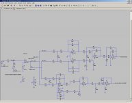
I have designed a new IV converter, which I'm going to build, same gain and impedance as the datasheet one but one order less.
I have simulated on LTspice a 1-bit DAC (w/o RTZ as I'm not able to model).
Datasheet says 4.4V min VOH digital output (@20uA). Mmmm too much. I will get more than 18Vpp at the AC output. Unless output voltage VOH will go down if more current will be required at the output (like in this schematic @1.6mA)...but I don't think less than 3.5V
How I can read this?
Attachments
The datasheet is indeed very unclear about the impedance of the return-to-zero DAC outputs.
However, the output drivers are essentially CMOS logic gates supplied by pins VA1, VA2, VA3 (nominally +5 V) and AGND1, AGND2, AGND3 (nominally 0 V). CMOS logic gates usually have output resistances between 10 ohm and a few hundred ohm and when they are not loaded, they switch all the way from supply to ground.
In this case, the output resistance must be much smaller than the 1.21 kohm series resistors the Crystal/Cirrus people use in their figure 16. The output resistances with output high and with output low won't match well, because the resistance with output high depends on a PMOS on resistance and with output low on an NMOS on resistance. They have to swamp this effect with a much bigger series resistance to prevent the problem I mentioned in my earlier post.
So all in all, the outputs switch between 0 V and 5 V when they are not loaded and they have an output resistance that is much smaller than 1.21 kohm, so the levels won't drop much when you connect your filter.
I have the impression that you use a PWM generator as a model for the sigma-delta in your simulation. If you drive it all the way, you'll get a larger maximum level than you'll get in reality. Single-bit sigma-delta modulators with an order greater than two are usually only driven from 25 % ones/75 % zeros to 75 % ones/25 % zeros. On top of that, you have 25 % signal loss due to return-to-zero coding. All in all, each RTZ DAC output will have a voltage that averaged over a few hundred clock cycles will vary between 0.75 * 0.25 * 5 V and 0.75 * 0.75 * 5 V.
By the way, VA1, VA2, VA3, AGND1, AGND2 and AGND3 will have to be very clean and well-decoupled to get a low noise floor and low distortion.
Last edited:
You are totally right!
And I even tested it...
I don't know how to exactly simulate Delta Signma 1-bit RTZ PWM to turn the information into a pulse with modulated output
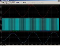
but if I sample in my above LTspice test with a reduced duty cycle (3/4) triangle wave (44.1KHz x 8, period=28us, t_rise=10.5us, t_fall=10.5us, t_on=0, t_off=7us) instead of a full triangle wave, I obtain a reduced Vpp converted AC signal. Vpp is now 11V, that is 3.9 VRMS.
The waveform of the recontructed output AC signal is as good as it was before by using a "full" triangle wave sample.
In any case, before your kind clarification, I had also simulated the IV analog filter of the Philips_CDI_220_(60,61,65,77)_Service_Manual which is using CS4303 and the gain is exacly the same as the one in the datasheet, which is, hence, equal to the one I have designed.
I'm going to test my design in the next couple of months and I hope to post here the results.
Many thanks to have illuminated me!

And I even tested it...
I don't know how to exactly simulate Delta Signma 1-bit RTZ PWM to turn the information into a pulse with modulated output
but if I sample in my above LTspice test with a reduced duty cycle (3/4) triangle wave (44.1KHz x 8, period=28us, t_rise=10.5us, t_fall=10.5us, t_on=0, t_off=7us) instead of a full triangle wave, I obtain a reduced Vpp converted AC signal. Vpp is now 11V, that is 3.9 VRMS.
The waveform of the recontructed output AC signal is as good as it was before by using a "full" triangle wave sample.
In any case, before your kind clarification, I had also simulated the IV analog filter of the Philips_CDI_220_(60,61,65,77)_Service_Manual which is using CS4303 and the gain is exacly the same as the one in the datasheet, which is, hence, equal to the one I have designed.
I'm going to test my design in the next couple of months and I hope to post here the results.
Many thanks to have illuminated me!
Attachments
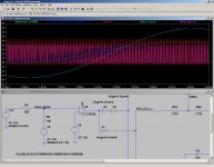
I doubt if it will help you and sigma-delta modulators are notoriously difficult to simulate accurately anyway, but if you should want to include a real sigma-delta in the simulation, there are two ways to do it:
1. Use a separate program to make a sigma-delta modulate and import it into a PWL source. I can modify a Pascal program I have for you if you like.
2. Include an analogue sigma-delta modulator (that is, a sigma-delta ADC without the digital filter) in the simulation and go from analogue to sigma-delta modulate and back to analogue.
You can find a schematic of a 64 times oversampling sigma-delta modulator, albeit not a very good one, in this post:
https://www.diyaudio.com/forums/dig...-dsd-adc-op-amps-logic-gates.html#post5425021
A return-to-zero DAC is simply a logic gate that blocks the signal during a part of each clock cycle. In the CS4303 it blocks the signal during one quarter of each period. You could model that with a fast CMOS AND gate of which one input is kept low from one-eight period before until one-eight period after the moment when you expect the other input to switch.
By the way, the transient analysis data compression feature that is on by default in LTSpice can totally mess up the spectrum of the simulated signal.
- Status
- Not open for further replies.