ClearPath: an ESS DAC project FPGA based
Hi folks,
I have the pleasure and the excitement to present my first project on the pages of this forum. Its name is ClearPath.
It's a project that I had in mind for a long time, more than 6 years ago, but alas I did not find the time to finalize it before now. It is a DAC, based on the famous ESS chip ES9018 (it could also use the latest ES9038PRO. I still have not tried it, although I signed the NDA and I have the datasheet).
It has the following features:
The Zynq with its ARM has a computing power that can be used to develop an entire very advanced DSP audio.
This is one of the interesting aspects of the project, though it has the cost of the FPGA daughterboard.
The other is given by the particular configuration of the power supply, which is inductive. It is characterized by the fact that L is an energy storage element and it has the following advantages:
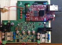
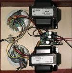
Attached you can see an high level architecture, an image of the board, and a picture of the power supply. The boards are still without a box, and are mounted on wooden bases.
In a next post, while I'm awaiting your impressions, I'll publish the schematics.
Update 1st June 2017
DoP and DoPE decoder added into FPGA. Now the DAC is capable to play DSD64 and DSD128 from USB and DLNA interfaces. The decoding process is done directly into FPGA. That it is independent from the DAC chip and it works with both the ES9018 and the ES9038.
Bye,
Isidoro Orabona
Hi folks,
I have the pleasure and the excitement to present my first project on the pages of this forum. Its name is ClearPath.
It's a project that I had in mind for a long time, more than 6 years ago, but alas I did not find the time to finalize it before now. It is a DAC, based on the famous ESS chip ES9018 (it could also use the latest ES9038PRO. I still have not tried it, although I signed the NDA and I have the datasheet).
It has the following features:
- You can connect to the source via SPDIF AES/EBU, asynch USB or Ethernet
- the analog and digital domains are galvanically isolated
- the power is inductive, with an upstream shunt regulator (later I will explain why I did this choice)
- the output can directly control headphones
- uses a low jitter clock (obviously). I chose to use quartz at 45.1584 and 49.152 MHZ
- includes a Zynq FPGA with an ARM Cortex-A9 where the programmable logic and firmware resides
- the usb stack is developed by me, starting from a xilinx driver, as well as the ChibiOS/RT port on Zynq (I'm the coauthor of a ChibiOS anchestor)
- the TCP/IP stack is now based on lwip2.0, which I ported under ChibiOS
- the DLNA interface is based on an open stack of Intel, revised and adapted by me (it was tremendously buggy)
The Zynq with its ARM has a computing power that can be used to develop an entire very advanced DSP audio.
This is one of the interesting aspects of the project, though it has the cost of the FPGA daughterboard.
The other is given by the particular configuration of the power supply, which is inductive. It is characterized by the fact that L is an energy storage element and it has the following advantages:
- it avoids current spikes in the rectifiers and in the capacitors during the charging cycle
- the rectifiers conduct for a whole electrical cycle with a peak current near the average
- thanks to this, it shows low radio frequency emissions and rectification disturbances, even if it can worsen low-frequency electromagnetic emissions.
- it keeps virtually constant power impedance from electric network point of view, and the current circulation doesn't adruptly change during network cycle
- has a marked filter action and the ripple residue has a low harmonic content; it's almost perfectly sinusoidal
- there is a very low stress of the electrolytic filter capacitors and then it extends their life cycle
Attached you can see an high level architecture, an image of the board, and a picture of the power supply. The boards are still without a box, and are mounted on wooden bases.
In a next post, while I'm awaiting your impressions, I'll publish the schematics.
Update 1st June 2017
DoP and DoPE decoder added into FPGA. Now the DAC is capable to play DSD64 and DSD128 from USB and DLNA interfaces. The decoding process is done directly into FPGA. That it is independent from the DAC chip and it works with both the ES9018 and the ES9038.
Bye,
Isidoro Orabona
Attachments

Last edited:
As always, there is a good ES9018 project shown and almost no users are interested to comment.
As a soldering freak, I see some imperfections like blue pots, radiators and some strange bridge at U18 (?). But overall, the board looks very nice. Good you used small caps near the DAC (0402?), but I'd place the bigger caps on left and right a little closer. Although, they are closer than on the Prometheus board 😛
How many shunts are there on the board?
I like the fact that the clock path is very short and seems to be not distracted by other signals. If I would change one thing, I'd separate the ground plane for clock signal feeding DAC chip and connect to other ground planes only with chokes.
And, finally someone intends to use the programming good of ES9018 chip with FPGA CPU.
Thank jot23 for your interest and your suggestions.
The 'small caps' are 3 terminals EMIFIL (NFM18PS) in 0603 package. I found them to be more critical than the bigger ones (that are C0G): the EMIFILs are on the 1.2V core vdd, while the C0G on avcc. Therefore in the layout I gave priority to them, and the space has served for the 1.2V plane below them (the board has 4 layers).
There are two shunt, one on each main power rail (+ and -).
The clock has however his own filter with ferrite and emifilters, and yes you are right, no other signal runs close to it.
I don't like those imperfections either (they annoy me). Unfortunately, I had to rework by hand the heatsinks, because of the bad soldering in the reflow oven (they were overzealus in doing their job 🙂 ).
Last edited:
ClearPath DAC schematic and use case
Hi,
I attached the ClearPath DAC schematic, together with a slide showing the DAC used as a DLNA Media Renderer. The schematic pdf has popup menu on the components for the details.
Any suggestion or comment is welcome.
Isidoro
Hi,
I attached the ClearPath DAC schematic, together with a slide showing the DAC used as a DLNA Media Renderer. The schematic pdf has popup menu on the components for the details.
Any suggestion or comment is welcome.
Isidoro
Attachments
Very nice project!
One thing I did notice on the schematic is that you seem to be pulling up the SDA line but not SCL (on the clean side). Is everything working OK regardless of that?
One thing I did notice on the schematic is that you seem to be pulling up the SDA line but not SCL (on the clean side). Is everything working OK regardless of that?
Hi Dimdim,
everything works OK. The Si8602 has an unidirectional channel for SCL made by a standard CMOS input. Therefore the (hidden) pullup that I programmed in the OBUF of the FPGA allows everything to work fine.
Bye,
Isidoro
everything works OK. The Si8602 has an unidirectional channel for SCL made by a standard CMOS input. Therefore the (hidden) pullup that I programmed in the OBUF of the FPGA allows everything to work fine.
Bye,
Isidoro
Exceptional piece of Engineering work
I'm definitely interested. How did you do all of this all by yourself?
I think the firmware alone is so much work. I would really love to see
it work with ES9038pro.
Thanks for sharing.
I'm definitely interested. How did you do all of this all by yourself?
I think the firmware alone is so much work. I would really love to see
it work with ES9038pro.
Thanks for sharing.
there is a real dearth of good multichannel DACs done right.
Hopefully there is a path to that here.
Hopefully there is a path to that here.
ESS9038PRO
Me too 😉. Thanks for your interest.
I would like to gather a significant number of people interested in, before working to the design again. I would be happy if I could define a kit that allows anyone to build it. The ESS9038PRO is easily adaptable changing very few components, but maybe it deserves a separated project in order to get the best from it.
There are several things that should still be done in the current design:
Bye,
Isidoro
I'm definitely interested. How did you do all of this all by yourself?
I think the firmware alone is so much work. I would really love to see
it work with ES9038pro.
Thanks for sharing.
Me too 😉. Thanks for your interest.
I would like to gather a significant number of people interested in, before working to the design again. I would be happy if I could define a kit that allows anyone to build it. The ESS9038PRO is easily adaptable changing very few components, but maybe it deserves a separated project in order to get the best from it.
There are several things that should still be done in the current design:
- the LCD display interface (I setup the hw interface, it needs the firmware, that it is nothing compared to all the firmware already developed)
- the firmware for a Pmod wifi module
- the remote control and a digital volume knob (via an encoder) to use when the DAC is not used as a DLNA DMR
Bye,
Isidoro
Isidoro
All I can say is wow! That's a very impressive effort. I am mostly an analog electronics person so I am in awe of your digital design and programming knowledge. I think you would get more traction on here if the project specifically targeted the 9038. There is a lot of positive buzz about the 9038 now that commercial products are being evaluated. Folks are more likely to sign on to a project where the latest Dac chip is featured.
I for one am interested and will be following your progress.
Last edited:
Thanks for sharing. A very nice design indeed.
Love the synchronous mode with 45.1584 and 49.152 clocks.
Love the synchronous mode with 45.1584 and 49.152 clocks.
In the block diagram, you show an I/V stage. How/why did you choose this? To the best of my knowledge, the ES9018 is voltage out.
In the block diagram, you show an I/V stage. How/why did you choose this? To the best of my knowledge, the ES9018 is voltage out.
The ES9018 analog output is a differential current output equivalent to a voltage source with approximately 780Ohm in series. The full scale out is 3.9mA pp.
Cheers,
Isidoro
Nice work, except for the tantals - why use conflict minerals?
I agree! I already planned to substitute them with polymer aluminium caps, hoping that I don't lose their damping action.
Conflict materials ... get real!
All you bloody Europeans and your pretentious, politically-correct ideologies!
I'm from the US of A and Trump is my prez...nicely dissolving decades of rubbish EPA protectionism.
...And I want all that poisonous Pb back in my solder so I don't have to landfill my device 'cause it stopped workin'!!
Yeah and toss out your Smartphones and iPads while you're at it.I agree! I already planned to substitute them with polymer aluminium caps, hoping that I don't lose their damping action.
All you bloody Europeans and your pretentious, politically-correct ideologies!
I'm from the US of A and Trump is my prez...nicely dissolving decades of rubbish EPA protectionism.
...And I want all that poisonous Pb back in my solder so I don't have to landfill my device 'cause it stopped workin'!!
Wouldn't that take quite a bit more space though? Very impressed with this project btw!I agree! I already planned to substitute them with polymer aluminium caps, hoping that I don't lose their damping action.
- Status
- Not open for further replies.
- Home
- Source & Line
- Digital Line Level
- ClearPath: another ESS DAC project