Building new board, ES9023 master clock questions
I am relatively new to designing DAC playback, but not new to design and software. The new board is for various purposes including sound effects for my product, which includes voice prompts etc. I added a PLL1708 clock for the master so that I would have selectable options to feed the ES9023. The board will playback 16 or 24bit stereo audio from an SD card only, and a processor that manages reading the data and sending to the DAC.
There is no real discussion in the ES9023 datasheet about what the master clock is doing relative to the lrclk, bitclock, and sdi, hopefully someone with experience can tell me what the relationship is and how the device handles async with no mode to change from snc to async? It only states what is "acceptable" for mclock speed. I routed the PLL1708 clock outputs sck2 and sck3 back to the processor. sck0 and sck1 feed the 9023, the software can choose which is enabled:
SCKO0: 768 fS(fS= 44.1 kHz)
SCKO1: 768 fS, 512 fS, 384 fS, 256 fS(fS= 48 kHz)
Clk to the processor: 256fs or 384fs @ selectable samplerate.
I am starting to sort out the I2S coding, but there is not a great explanation in the 9023 dsheet. My assumption is, that the 9023 can have the 768fs clk feeding it with no sync to the processor, just let the processor output the bitclk, sdi, and lrclk as it wants in async. Otherwise, I will attempt to bring the or 384 into the code for syncing the data.
I also wonder at what point that data is latched to the DAC output stage from the shift registers, leading edge of lrclock or trailing edge?
Thanks for any suggestions.
Last edited:
ESS has an app note which supplements the white paper ESS provides in their site's downloads section and US patent 7436333. It's available through the usual ESS document request process, though your distributor may have to get you in touch with ESS support directly. The short answer is so far as clock domain management goes ESS DACs are AD1955s with a first order interpolating sample and hold block bridging SCK and MCLK rather than zero order.
Thanks for the info. I got my first DAC board built yesterday and now am trying to sort out the ASM code to read the SD card and play back to the 9023. I have a PLL1708 with a 27m xtal, the DAC can see 768*44100 or 768*48k. The processor gets either 384*44.1k or 384*48, with an optional 256x if needed.
I am trying to find out the best way to clock the processor data writes to the DAC after each buffer transfer from the SD card. I must send 24bits even if lessor, so that means 48 bitclocks per sample. With a master clock at 384 x sample rate, 384/48 = 8 so that I can count every 8 clocks to set the bit clock high, or rather 5 clocks for low and 5 for high. I hardwired the DAC for I2S, so I must change the Word Select at bit 23 for the write to signify the LSB and MSB change. What I wanting to find out is what is the critical factor for the DAC buffer to shift out the data to the output. I assume the bit 23 of the Word Select is forcing the transition for shift out the data from shift register to DACoutput. So in other words, the earlier data could have arrived earlier or even at varying bitclock rates prior to bit 23, but the bit23 is the true timing concern to fire the DAC output.
Anyone have any knowledge if this is correct?
Attachments
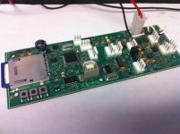
Sorry I uploaded the wrong image, here is the board.
RTC engine real time clock
Propeller Processor
PLL1708 clock
ES9023
THATcorp 2162 Dual VCA optional/patch or jumper in
OPA2134 op aps optional/patch or jumper in
OPA2134 opamps for VCA gain/atten
SD card
FT2323 USB
RTC engine real time clock
Propeller Processor
PLL1708 clock
ES9023
THATcorp 2162 Dual VCA optional/patch or jumper in
OPA2134 op aps optional/patch or jumper in
OPA2134 opamps for VCA gain/atten
SD card
FT2323 USB
Attachments
- Status
- Not open for further replies.