Your's is an example of where the WORD ground is being misused and leads to unsafe practice.
Ban the WORD ground.
Replace it with the correct term so that the user and everyone understands what is being referred to.
you always smart what anyone can say to you... please be more helpful for others not your ego ,
and please explain yourself why is word ground not valid after 200 years of usage (i am not native eng so maybe i misunderstanded you in that case i apologise)
If we gave a unique name and a unique route for EVERY return route of a two wire circuit connection, most of the "grounding" problems would disappear.
It's the confusion caused by naming everything as "ground" that allows the "thinking" that all these points are the same and at the same voltage and that they can simply be haphazardly joined together that creates many of the wiring errors.
Most "GND" are NOT at the same voltage.
No matter what AJT says about
a ground is a ground is a ground and a ground, 0 volts point....
Last edited:
Not only Ground (Return) structure, also low inductive and priority connections should be included in a schematic.
All signal, supply, return, and reference connections (notice how I avoided the use of the G word
") ) are important and you will always have to make tradeoffs in the routing.
) are important and you will always have to make tradeoffs in the routing. The schematic documents the circuit. I'm fine with layout notes on the schematic, but anything beyond that usually ends in a hair ball mess that is useless for layout and useless as documentation. Good layout requires a good layout engineer to translate the schematic into the actual circuit. Circuit = layout + components.
That's my view anyway.
~Tom
This is a great plan. What would you suggest?If we gave a unique name and a unique route for EVERY return route of a two wire circuit connection, most of the "grounding" problems would disappear.
GND = power input connector power connection.
GND_PWR = the "star" ground in the ground plane where the HF decoupling and Zobel network come together.
GND_LOAD = the speaker (-) connection (assuming single-ended, not bridged operation).
GND_REG = ground plane for the regulated supply for op-amps driving the chip amp (if applicable).
Referring to this schematic (neglect the L and C used for the loop gain sim),
R1 should terminate on GND_REG. GND_REG connects to GND_LOAD via a low-impedance (i.e. low resistance and low inductance - think a wide pour) connection. Parasitic inductance here will result in a rise in THD at HF (yes, I have measured data to back this up).
GND connects to GND_PWR and GND_LOAD via a ground plane (again, low inductance, low resistance).
If the LM3886 is used stand-alone (i.e. no driving op-amp or DC servo), R1 can terminate via a low-impedance trace to GND_LOAD.
This takes care of the board.
Now for the mains connection:
GND_EARTH is the green (yellow/green in the EU) wire ground from the mains inlet. This MUST connect directly to the (metal) chassis. This is for safety and required by code in most countries. If a plastic chassis is used, GND_EARTH must be connected to any metal parts that can be accessed by the user.
If using a differential input on the amp, life is simple as GND can connect directly to GND_EARTH. For a single-ended input, some use ground loop breakers connected between GND_EARTH and GND.
For a differential input using XLR connectors, pin 1 of the input XLR should connect to GND_LOAD. The pin 1 ground is just to establish the common-mode voltage between the source and the amp. It is not a safety ground and should never conduct any appreciable current.
~Tom
GND_PWR = the "star" ground in the ground plane where the HF decoupling and Zobel network come together.
GND_LOAD = the speaker (-) connection (assuming single-ended, not bridged operation).
GND_REG = ground plane for the regulated supply for op-amps driving the chip amp (if applicable).
Referring to this schematic (neglect the L and C used for the loop gain sim),
An externally hosted image should be here but it was not working when we last tested it.
R1 should terminate on GND_REG. GND_REG connects to GND_LOAD via a low-impedance (i.e. low resistance and low inductance - think a wide pour) connection. Parasitic inductance here will result in a rise in THD at HF (yes, I have measured data to back this up).
GND connects to GND_PWR and GND_LOAD via a ground plane (again, low inductance, low resistance).
If the LM3886 is used stand-alone (i.e. no driving op-amp or DC servo), R1 can terminate via a low-impedance trace to GND_LOAD.
This takes care of the board.
Now for the mains connection:
GND_EARTH is the green (yellow/green in the EU) wire ground from the mains inlet. This MUST connect directly to the (metal) chassis. This is for safety and required by code in most countries. If a plastic chassis is used, GND_EARTH must be connected to any metal parts that can be accessed by the user.
If using a differential input on the amp, life is simple as GND can connect directly to GND_EARTH. For a single-ended input, some use ground loop breakers connected between GND_EARTH and GND.
For a differential input using XLR connectors, pin 1 of the input XLR should connect to GND_LOAD. The pin 1 ground is just to establish the common-mode voltage between the source and the amp. It is not a safety ground and should never conduct any appreciable current.
~Tom
Last edited:
Pin1 goes to Chassis right at the connector.........................
For a differential input using XLR connectors, pin 1 of the input XLR should connect to GND_LOAD. The pin 1 ground is just to establish the common-mode voltage between the source and the amp. It is not a safety ground and should never conduct any appreciable current..............
The screen attached to the Pin1 (at both ends) can and does carry appreciable current.
To repeat what Andrew just wrote.......................................
For a differential input using XLR connectors, pin 1 of the input XLR should connect to GND_LOAD. The pin 1 ground is just to establish the common-mode voltage between the source and the amp. It is not a safety ground and should never conduct any appreciable current.
~Tom
In an XLR interconnect system, pin #1 is the shield and should be connected to the chassis (and only to the chassis) very near it's chassis jack. In some conditions, some experts say that the receive end cable shield need not be connected.
Any other way leads to the dreaded "Pin 1 Problem" which by the way applies to all shielded cables.
Your schematic has 5 GND's, the TI schematic has 7. A PCB designer can randomly place the components, add a GND plane, join the remaining dots and honestly say he kept to the original design.
A crappy PCB designer will do just that. Connect the dots, call it done. A good PCB designer will keep the current flows in mind and route the board accordingly. If the PCB designer is savvy enough to understand the circuit, he could do that on his own. If the PCB designer is not savvy enough, he'd have to read the layout notes on the schematic and work with the circuit designer to achieve the desired performance. I go through these layout-design iterations every day at work, albeit, on an IC level rather than board level.
In an XLR interconnect system, pin #1 is the shield and should be connected to the chassis (and only to the chassis) very near it's chassis jack. In some conditions, some experts say that the receive end cable shield need not be connected.
Any other way leads to the dreaded "Pin 1 Problem" which by the way applies to all shielded cables.
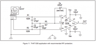
And to repeat my previous statement: Pin 1 must refer to circuit ground, somehow. Otherwise, the input common-mode voltage is not controlled. If the source and the receiver are plugged into two different mains phases, you could have hundreds of volt of common-mode difference. The differential receiver won't like that too much. I suggest reading the THAT1200 differential receiver data sheet. I've attached the relevant figure for those too lazy to click on the link.
In most amps, the supply return is connected to the chassis at one point. That forms the Pin 1 reference.
~Tom
Attachments
And I would suggest reading more about that dreaded pin #1 problem.
in the 'Hum, Buzz, and RF Interference' section.
Audio Systems Group, Inc. Publications
******************************************
Or do a search for the 1995 Neil Muncy paper that AES 48 is based on.
"Noise Susceptibility in Analog and Digital Signal Processing Systems"
NElL A. MUNCY, AES Member
**********************************
Or if you are interested in how it's done in big multi-building movie or TV studios, see:
Tony Waldron's Audio & EMC ranting and ravings
http://www.fragrantsword.com/twaudio/
Last edited:
Hi,
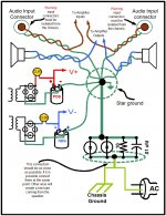
I have been following this thread for a while and I didn't want to get involve because I hated ground problems. Any way I already built 3 lm3886 and all have been hums free. All have 1.8 mv volts output offset and the sound it is super excellent. So attached it is a drawing that successfully I used to wired my amplifiers with good results. Just use it as a reference and hoping it will help you to fix your ground problem.
I have been following this thread for a while and I didn't want to get involve because I hated ground problems. Any way I already built 3 lm3886 and all have been hums free. All have 1.8 mv volts output offset and the sound it is super excellent. So attached it is a drawing that successfully I used to wired my amplifiers with good results. Just use it as a reference and hoping it will help you to fix your ground problem.
Attachments
XLR Pin1 goes to Chassis. End of story......................
And to repeat my previous statement: Pin 1 must refer to circuit ground, somehow. ................
Would you define "hum free" for me/us?................. Any way I already built 3 lm3886 and all have been hums free. All have 1.8 mv volts output offset ..............
Connect shorting plugs to the two Inputs.
Measure the mVac and mVdc at each output.
Connect a pair of normal coaxial interconnects to the Inputs.
Connect the barrels of the far ends together, as they would be in a stereo Source.
Add shorting links to the far ends of both interconnects.(an assistant can do this by just shorting the pins and barrels of the two interconnect ends).
Measure the mVac and mVdc at each output.
Post the results of the 8 measurements.
- Status
- This old topic is closed. If you want to reopen this topic, contact a moderator using the "Report Post" button.
- Home
- Amplifiers
- Chip Amps
- Help:Transformer on 3886 chipamp overheating!