Hi all,
since I'm relatively new in building amps, I'm here for some advice.
My plan is to build a single channel amp around the TDA2040 chip, I don't really need too much power as the amp will be used to drive a near field mini monitor at low to medium SPL. I already have a 50VA 9V toroidal transformer with 2 secondary windings that will be connected in series with a center tap thus providing -9, 0 9V or roughly -12, 0, 12V after rectification. I know that I can use higher voltages with this chip but this is what I have and for now I don't want to buy another transformer, I can do that later.
First question: what should I use as a smoothing cap after the bridge rectifier. 2x 2200uF? 4x 2200uF? some other values?
Second question is about the heatsink. The tab of the chip is connected to the pin 3 and with a split power supply this pin is connected to -V. I don't have any experience on that but I'm pretty sure I do need to (electrically) insulate the heatsink. What is the proper method of doing that? Is thermal grease between the tab and the heatsink sufficient, or do I need to use a thermal pad, or other method that I'm not aware of?
Third question is about power-on or off pop up. Does this chip provide some protection on that or do I have to worry about? What I have to do?
Last question is about the PCB. Following the datasheet I've designed the attached PCB. Does it seems good, or are there flaws that I'm not aware of? Also what happens if I change C3, C4 and C7 to 0.15 or 0.22uF (instead of 0.1uF)? Or if I change R4 to 2R2 instead of 4R7? Or R2 to 560R instead of 680R?
Any other comment will also be appreciated.
The datasheet of the TDA2040 can be seen here: Datasheet
Thanks in advance, Ralf
Attachments
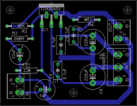
You have correctly separated the Signal side from the Power side. Good.
But go further: add pads for a Signal Ground to Power Ground combination of paralleled resistor & two inverse parallel diodes. There's plenty area at the bottom of your proposed PCB. You can link out this option if you build a true monoblock.
You have connected the Speaker Return to the Power Ground. This makes the junction in there (on the PCB), the Main Audio Ground (MAG). You MUST use this as your MAG if you build a stereo or multichannel amplifier. Even a dual mono must use this MAG (this becomes impossible because you end up with two MAGs that are non-coincident).
Add RF attenuation to the input.
Reduce the loop areas of all the signal pair traces.
Reduce the loop areas of the Power input.
Reduce the loop area of the Zobel.
Reduce the loop area of the Speaker feed.
Leave room to replace the input electrolytic with a plastic film capacitor.
Push the chip closer to the edge of the PCB, so that the heatsinks fits.
Add multiple holes/pads (different Pin Pitch) for every capacitor.
Move the chip decoupling to right next to the Power Pins.
Replace the film decoupling with X7R decoupling caps.
Add diodes to limit back emf from the speaker.
Add diodes to short out accidentally reversed power connections.
A circuit has a source voltage.
From that source voltage comes TWO wires.
I (and others) refer to these two wires as Flow and Return.
EVERY circuit has this Flow and Return.
The AREA included between the Flow and Return is an aerial.
This aerial emits radiation and it receives radiation.
Your layout should strive to minimise this radiation.
You do this by minimising the AREA enclosed by the loop formed between Flow and Return.
There is an alternative:
form a figure of 8 with the Flow and Return.
The first half of the loop sends out one phase of radiation. The next half sends out the opposite phase.
If the two loops are exactly equal and they are exactly the same distance from a receiver, then the two out of phase radiations cancel. This is why we see twisted pairs so often.
Every loop just about cancels with the adjacent loop in the twist.
You can't do this twisting with traces, at least not easily. Instead you can swap the traces from one side to the other to try to improve the cancellation via opposite phases. This is rarely seen, but Cherry described the technique and showed an example PCB in an old paper, about mid 90's.
Are your speakers 8 Ohms nominal?
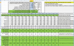
You can use any amount of reservoir capacitance. But the reservoir capacitance determines the RATED max output power (at the onset of clipping), and the maximum ripple voltage.
You might be better off not using a center-tapped arrangement and using two bridge rectifiers, instead. That would use the transformer a little more efficiently, if I recall correctly.
You might want to use Schottky diodes for rectification, to conserve voltage drop.
With such a low rail voltage, a lot will depend on exactly what the worst-case diode drop is, and also on what the chipamp's clipping voltage is (i.e. the minimum voltage between PSU and output), at your rail voltage.
Looking at the datasheet's plot of max output power vs rail voltage, it looks like the "vclip" voltage of the TDA2040 is about 1.5 Volts, when the rail voltage is around 11 Volts.
So, your peak secondary voltage (12.73 V), minus the two diode drops, minus the vclip of the chip, minus the maximum ripple voltage, will be your peak output voltage at the onset of clipping. To guarantee that clipping can't occur, even at the rated maximum output level, you should assume that the output is constant DC at the peak output level. Solving the capacitor-discharge (differential) equation with those conditions can give an algebraic equation for capacitance as a function of the corresponding max rated output power level or ripple voltage amplitude. I did that, a while back, and made a spreadsheet that provides a range of output power levels and gives the corresponding minimum reservoir capacitance for each one. I'll attach it. You will have to figure out what the diode drops will be at the maximum output current, and enter the correct number for that, since it will depend on what kind of rectifier diodes are used.
Remove the ".txt" from the end of the filename, to use the attached Excel spreadsheet file.
If you want to see what rated max output power you would get, for a particular capacitance value, single-click in any column's capacitance cell and then select Excel's "Data"-->"What If Analysis" option, and tell it to make the capacitance value what you desire, by changing the value in the "Rated/Theor (%)" row (the blue row) for that column. I have the capacitance values set for various combinations of 2200, 4700, and 10000 uF. But they will change if you modify the mains frequency or cap voltage rating field. So then you might want to reset them to convenient values.
Remember, too, that the capacitance and ripple voltage values are all for worst-case at max rated output power levels. You can use a lower reservoir capacitance, if you don't care what happens near the maximum output level.
Cheers,
Tom
Attachments
Last edited:
Tom,Are your speakers 8 Ohms nominal?
You can use any amount of reservoir capacitance. But the reservoir capacitance determines the RATED max output power (at the onset of clipping), and the maximum ripple voltage.
<snip>
thanks for your work. I downloaded your spreadsheet, and played a bit. The only problem is that from the datasheet it is difficult to choose a max rated power because the only graphs are for 0.5 and 10% distortion, and I'd design for a lower distortion. Probably for 0.1% the rated power is about half of the max theoretical one, and from that given only 1 8Ohm channel, I can use without problems what I already have (4700u 50V caps).
Thanks again
Ralf
Andrew,
about your suggestions, some were straightforward, but for others I have some questions.
There is a reference for a RF protection at the input, but what is needed is only the 220pF cap (C2 in the Figure 1), or also the two 2K2 R1 and R3 resistors?
For this I have seen different things.
Rod Elliott writes for his project: "Note that the speaker must return to the central 'star' earth (ground) point. If connected to the amplifier's earth bus, you will get oscillation and/or poor distortion performance."
The SGS datasheets for the TDA2040/2050 show a split power supply PCB without a specific ground pin for the speaker (and there is for a single supply PCB). On the other hand the NS datasheet for the LM1875 does show a specific ground pin for the speaker marked as -Vout.
So can I connect the Speaker Return to the Power Ground (option 1), or is better to return the speaker to a central ground point (right after the rectifier/caps) (option 2)? Consider that my amp will drive a FM tuner that uses the same DC power, in case of the option 1 do I need to connect the tuner ground to the MAG?
Thanks,
Ralf
about your suggestions, some were straightforward, but for others I have some questions.
I think you meant to move the C3 and C4 0.1uF caps near the pin 5 and 3 respectively (for a short as possible path from cap to pin). Is that correct?Move the chip decoupling to right next to the Power Pins.
I think you are referring to the C3 and C4 caps. What's the reason to replace them with X7R ceramic caps?Replace the film decoupling with X7R decoupling caps.
That I don't know how to do it, because I wasn't able to find detailed references. What I found is a project from Rod Elliott for a LM1875/TDA2050 chip, which have the same pinout of the TDA2040: Single Chip 25W Amplifier (Project 72)Add RF attenuation to the input.
There is a reference for a RF protection at the input, but what is needed is only the 220pF cap (C2 in the Figure 1), or also the two 2K2 R1 and R3 resistors?
You have connected the Speaker Return to the Power Ground. This makes the junction in there (on the PCB), the Main Audio Ground (MAG). You MUST use this as your MAG if you build a stereo or multichannel amplifier. Even a dual mono must use this MAG (this becomes impossible because you end up with two MAGs that are non-coincident).
For this I have seen different things.
Rod Elliott writes for his project: "Note that the speaker must return to the central 'star' earth (ground) point. If connected to the amplifier's earth bus, you will get oscillation and/or poor distortion performance."
The SGS datasheets for the TDA2040/2050 show a split power supply PCB without a specific ground pin for the speaker (and there is for a single supply PCB). On the other hand the NS datasheet for the LM1875 does show a specific ground pin for the speaker marked as -Vout.
So can I connect the Speaker Return to the Power Ground (option 1), or is better to return the speaker to a central ground point (right after the rectifier/caps) (option 2)? Consider that my amp will drive a FM tuner that uses the same DC power, in case of the option 1 do I need to connect the tuner ground to the MAG?
Thanks,
Ralf
I think you have your answers correct.
x7r seem to have the appropriate amount of damping resistance (ESR) and low enough inductance that adding them to the supply rails does not make rail oscillation worse and usually much better.
For grounding go and read
Audio Component Grounding and Interconnection - diyAudio
if you can't understand my suggestion.
Answering one of my own questions.
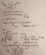
What happens changing the R2 resistor to 560 from 680 Ohm: gain goes up from 27.4 dB to 28.5 dB.
With the NF divider using 22K and 560 ohms, I get 32.1db V gain. How did you arrive at your figures?
- Status
- This old topic is closed. If you want to reopen this topic, contact a moderator using the "Report Post" button.
- Home
- Amplifiers
- Chip Amps
- Questions about a TDA2040 based amp