Hi,
I got this amplifier and i am struggling for few days now to repair it...
Let's start with beginning: When i firs got it i found out that power supply is shorted and i measured power supply FET's , 11 out of 16 dead, so removed all of them . (There are 2 transformers on the power supply side, 2 banks for each transformer).
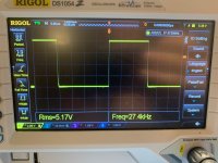
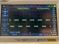
I then measured the square wave on all banks, all good like in attached pictures.
I then moved to the amplifier section, found out few dead FET's, removed all of them , then placed one FET on each bank from the power supply and powered up... Rail voltage climbed up for both rails, but.... too much current was drawn from the power supply ( > 8 Amps) and 2 of the power supply FET's heating up very quickly...
Next step was to remove rectifiers just to isolate the power supply, same problem...
I then changed FET's between sides, problem din't move with the FET's, it's on the same side.
I measured transformers coils with a cheap component tester, they are showing about the same value of inductance ...
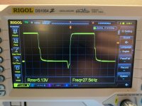
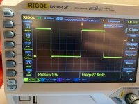
I attached pictures with the square wave without FET's for both sides and Square wave with FET's attached for both sides.
I will refer to A as the good side and B as the bad side. It's visible that the square wave on the B side is wrong after FET's are attached, while looks OK with FEt's removed.
Do you have any idea? Can be the driving IC? Or the buffer transistors which may be fine with no load, but may go crazy when they actually need to drive the FET's?
i need also to mention that the side which is heating the FET's had more damage than the other one.
Any suggestion are welcome....
thanks in advance for helping!
I got this amplifier and i am struggling for few days now to repair it...
Let's start with beginning: When i firs got it i found out that power supply is shorted and i measured power supply FET's , 11 out of 16 dead, so removed all of them . (There are 2 transformers on the power supply side, 2 banks for each transformer).
I then measured the square wave on all banks, all good like in attached pictures.
I then moved to the amplifier section, found out few dead FET's, removed all of them , then placed one FET on each bank from the power supply and powered up... Rail voltage climbed up for both rails, but.... too much current was drawn from the power supply ( > 8 Amps) and 2 of the power supply FET's heating up very quickly...
Next step was to remove rectifiers just to isolate the power supply, same problem...
I then changed FET's between sides, problem din't move with the FET's, it's on the same side.
I measured transformers coils with a cheap component tester, they are showing about the same value of inductance ...
I attached pictures with the square wave without FET's for both sides and Square wave with FET's attached for both sides.
I will refer to A as the good side and B as the bad side. It's visible that the square wave on the B side is wrong after FET's are attached, while looks OK with FEt's removed.
Do you have any idea? Can be the driving IC? Or the buffer transistors which may be fine with no load, but may go crazy when they actually need to drive the FET's?
i need also to mention that the side which is heating the FET's had more damage than the other one.
Any suggestion are welcome....
thanks in advance for helping!
Attachments
Hi Perry, and thank you very much for the quick reply,
Yes the 4th image is the drive wave with FET's attached on the B (wrong) side. In this case (PNP transistor damaged, or ground missing) it's possible that the square wave without FET's attached is still looking good?
I will check this later today when i get back home and will come back with conclusions. I have replacement transistors, so i can maybe replace all of them...
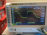
When the FETs are in the circuit, they introduce capacitance. After being charged by the NPN driver transistors, they must be discharged quickly. With defective PNP drivers, the discharging is slow which is why the falling part of the waveform isn't very nearly vertical (as it should be).
Thank you very much for helping, i changed all 8 drivers and it's working now. I used BD140 and BD139 for replacement. I am using for the moment 4 FET's that were surviving in the power supply, one on each bank, so i have a full functional power supply section.
But now i moved to the amplifier section... Here about half of the FET's are dead, so i removed all of them, but i don't have any square waves.
I tried also to use a 40 HZ tone on the input, but i can't see any switch. I know that most of the times the IC's on the driving board are dead, so i will order and change them, but i also want to order the other IC's and buffer transistors, maybe 2 big diodes as i can read a short on one of them...
Does anybody have an electrical schematic for this amplifier, as few IC's are scratched out, and on the small transistors i can't see what's their code?
Thank you again!
Hi everybody!
It's been a long time since last post, but finally the amplifier was fixed (i had to wait long time for parts delivery, due to some customs issues) ... and broken again ...
...
The parts changed on the driver board: both 21844s ICs , Diode D2, capacitor CL2 and IC U6 (LM293). I had a nice square-wave after i changed all the above, then i fitted up all power supply and amplifier transistor and everything was fine, nothing heated up, all good...
The problem is that i decided to add some silicon to the transformers and output filters... and even if they rested for few days the silicon didn't dried up and ... i don't need to explain too much ... i have problems again... on the power supply i burned just one transistor and its gate resistor, both changed and power supply is now OK (i still have power supply isolated from amplifier section) .
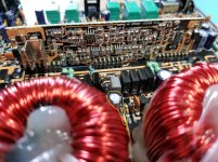
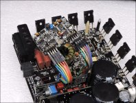
On the amplifier section transistor are OK, but i have a blown capacitor and diode ... the capacitor is C82 and diode is D51 ... Is anybody having a similar amp, or an electrical schematic so i can identify capacitor value, as its so bad blown that i can't read anything on it...
I have attached a picture to show the 2 parts.
It's been a long time since last post, but finally the amplifier was fixed (i had to wait long time for parts delivery, due to some customs issues) ... and broken again
...The parts changed on the driver board: both 21844s ICs , Diode D2, capacitor CL2 and IC U6 (LM293). I had a nice square-wave after i changed all the above, then i fitted up all power supply and amplifier transistor and everything was fine, nothing heated up, all good...
The problem is that i decided to add some silicon to the transformers and output filters... and even if they rested for few days the silicon didn't dried up and ... i don't need to explain too much ... i have problems again... on the power supply i burned just one transistor and its gate resistor, both changed and power supply is now OK (i still have power supply isolated from amplifier section) .
On the amplifier section transistor are OK, but i have a blown capacitor and diode ... the capacitor is C82 and diode is D51 ... Is anybody having a similar amp, or an electrical schematic so i can identify capacitor value, as its so bad blown that i can't read anything on it...
I have attached a picture to show the 2 parts.
Attachments
Check in the picture here:
Ground Zero GZPA 1.4000DXII - AMP Performance
and here
Emphaser EA 13000SPL - AMP Performance
If you can find it.
Ground Zero GZPA 1.4000DXII - AMP Performance
and here
Emphaser EA 13000SPL - AMP Performance
If you can find it.
Thank you very much Perry for your answer.
I know exactly when the capacitor blown. As i said in my previous post, one resistance and one transistor failed on the power supply side(i don't know which failed first) ; the cap blew away just after the power supply 47 ohm gate resistance burned open.
Now power supply is fixed, so hopefully just by replacing the cap and maybe the diode (i need to measure it first) will fix it...
Perry, can you please explain me what is that part of the circuit for? I can't figure out... I see it's part o the protection circuit, but i don't know what the piece with C82 and D51 is really doing... i want to also understand why the capacitor exploded ...
I found out that the 5V6 diode is gone also, and i need to wait about 2 weeks to get it, so i have enough time to investigate more...
Thank you!
I found out that the 5V6 diode is gone also, and i need to wait about 2 weeks to get it, so i have enough time to investigate more...
Thank you!
They are part of the protection circuit but that's not their main function. The cap and resistors produce a slight delay in the turn-on of the driver ICs.
I see no way for that capacitor to explode from a fault in the circuit. The resistor values from the parts of the circuit that could have supplied enough voltage are too high to make it explode. That's why I suggested looking for loose wire strands that could have shorted to other sources of voltage.
I see no way for that capacitor to explode from a fault in the circuit. The resistor values from the parts of the circuit that could have supplied enough voltage are too high to make it explode. That's why I suggested looking for loose wire strands that could have shorted to other sources of voltage.
I don't use silicone for fixative but tested a couple of different types and they were not conductive but someone else had a problem with uncured silicone conducting but it was the silicone that smelled like vinegar. The ones I tested were the ones that did not smell like vinegar (or anything else).
Hi again! Now after Christmas break I turned my head to this again. I hope I will finish it by the next Christmas
So far, what I did yesterday:
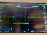
Changed the cap and the diode, turned on, nothing was heating, normal current drawing, but... Funny or no square wave( on one side it was a noisy square wave, on the other side noisy nothing). I removed all the amplifier FETs, but the square wave was still the same...
When I forced the driver board one side(which is now in headers) i started to have square wave on both sides... So probably I have a bad contact, I will probably remove the headers and solder the board directly...
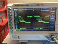
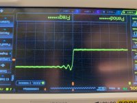
So far so good, I kind of have square waves on both sides, but they look funny, they're very noisy... I also placed a signal to the imput, and the square changed its amplitude to the signal frequency...
Any ideea what to check/change to get rid of the noise?
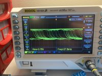
I attached picture with the wave, and also a zoomed picture to see its transition...
So far, what I did yesterday:
Changed the cap and the diode, turned on, nothing was heating, normal current drawing, but... Funny or no square wave( on one side it was a noisy square wave, on the other side noisy nothing). I removed all the amplifier FETs, but the square wave was still the same...
When I forced the driver board one side(which is now in headers) i started to have square wave on both sides... So probably I have a bad contact, I will probably remove the headers and solder the board directly...
So far so good, I kind of have square waves on both sides, but they look funny, they're very noisy... I also placed a signal to the imput, and the square changed its amplitude to the signal frequency...
Any ideea what to check/change to get rid of the noise?
I attached picture with the wave, and also a zoomed picture to see its transition...
In the future, if you have to remove the board (often, not necessary, even to replace ICs), I'd suggest using wire jumpers. They allow full access and don't have intermittent connections (which can cause the output transistors to fail, among other problems).
The best option are the Arduino breadboard jumper wires. They're dirt cheap and save a lot of time compared to stripping and tinning wires.
The best option are the Arduino breadboard jumper wires. They're dirt cheap and save a lot of time compared to stripping and tinning wires.
Attachments
- Status
- This old topic is closed. If you want to reopen this topic, contact a moderator using the "Report Post" button.
- Home
- General Interest
- Car Audio
- Ground Zero GZPA 1.4000DXII