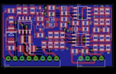
Hey folks, I am starting on another class D schematic and board clone. I'm calling this one the 3S type mini driver. It may not be made by 3S-Tech, but it is definitely a derivative of their design.
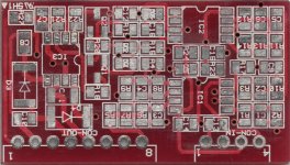
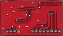
Anyhow, attached are low res imaged of the board. Linked are high res scans as well as the BOM I have so far worked out. I'm unsure of a few devices. D5 and D6 are both marked "F2". There are a lot of possibilities for this code. I believe it is a UDZS6.8B, 6.8V Zener diode in a SOD323 package. If anyone can confirm, that would be great, if not I will test one of the ones I pulled to see what it's zener voltage is. The other one is D3, it appears some of these boards just have a 2R2 resistor installed. Mine had a device marked 633A in this position. The closes I can find is SMCG5633A, that is a transient suppressor diode, however, according to the manufacturers datasheet the part should be marked 5633A, not 633A. So, jury is still out on this one. I used STPS4S200UF for D4 on mine, it is a 200V 4a Schottky diode, I think this one should be ok for most rail voltages, but you could go with a cheaper and lower voltage rated part if you have a smaller amp.
High Resolution Front (click)
High Resolution Back (click)
BOM (click)
Later,
Jason
Attachments
Here is the first draft of the schematic. I'll work on cleaning it up and doing board layout over the next few days. I still need to verify the zener voltage, but I will do that hopefully this afternoon. Please let me know if any errors jump out at you.
Schematic (click)
Later,
Jason
Schematic (click)
Later,
Jason
I tested the "f2" marked diodes. They are indeed 6.8v zeners, so the part listed in the bom/schematic should work just fine.
D3 is not a transient suppressor. I tested it and reverse biased it did not break down with the 40Vdc that I took it up to. Considering the one I thought it crossed to has a 18v breakdown voltage, I think we can safely assume it's not a TVS. It's got about a 0.6v forward voltage drop, so I'm thinking it's just a run of the mill rectifier.
Thanks,
Jason
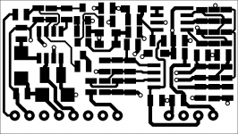
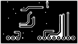
Board layout is done and passed DRC. I fixed a few errors in the schematic, so DL V2 below if you need it. Attached are toner transfer layouts. The PDF should have the best quality pictures. Size of the board is 1.625x.917 inches.
Schematic V2 (click)
Toner layout PDF(click)
Later,
Jason
Schematic V2 (click)
Toner layout PDF(click)
Later,
Jason
Attachments
Last edited:
- Status
- This old topic is closed. If you want to reopen this topic, contact a moderator using the "Report Post" button.