SO packages are indeed the easiest SMD packages to solder. I usually put a bit of solder on the tip of my iron, try to keep the IC in place and solder one corner pin with the solder on the tip. That's not the way you normally should solder anything, but it is just meant to fix the IC in place. I can then solder all other pins the normal way, and once that's done, resolder the first corner pin. For handsoldering SO packages it is handy if you can make the pads on the PCB a bit longer than strictly necessary.
By the way, if you want the absolute minimum noise and don't mind some extra complexity, there is a way to largely get rid of the noise of the 47 kohm termination: use a much higher resistance and put an amplified and inverted signal on its other side. The improvement is not very large: at most about 3 dB when there is no record playing, and much less when there is a record playing.
By the way, if you want the absolute minimum noise and don't mind some extra complexity, there is a way to largely get rid of the noise of the 47 kohm termination: use a much higher resistance and put an amplified and inverted signal on its other side. The improvement is not very large: at most about 3 dB when there is no record playing, and much less when there is a record playing.

Okay, I'm going to have a go... I've ordered a bunch of OPA1652AID and some SO-8 to 0.1" breakout boards - that way I can test my soldering ability and do a bit of experimentation with circuits before committing to a PCB design. I've also ordered some LME49710s to try out as well.
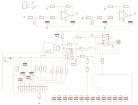
I probably should have started a new thread as this isn't really an LME49710 design any more... I've kept them for the DC smoothing networks but used OPA 1652s for the AC sections. Anyway if anyones got the time and inclination to give the schematic and layout a quick look I'd appreciate any comments / guidance.
I've run the circuit through TinaTi, it looks okay but I'm still learning the software.
Also I've split the RIAA filter caps up into smaller values in parallel so that I can get as close to the intended value as I can, I'll probably end up with some unpopulated spaces... is that a good idea? The gain is set to get about 1V from a 5.5mv MM cartridge.
Thanks,
Simon.
Attachments
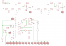
With a moving-magnet cartridge, the response between (say) 10 kHz and 20 kHz depends strongly on the capacitive load. Unless you know exactly what load capacitance your cartridge needs and what capacitance your cable has, it may be useful to include some spare capacitors and DIP switches so you can easily experiment with the load capacitance.
What types of capacitors do you use in the RIAA correction filter?
For the filter resistors I see you use SMDs. Thin film SMD resistors are generally better than thick film SMD resistors, they are more accurate and have less 1/f noise (which is mainly a concern for resistors that have a significant DC bias voltage across them, because without voltage across it it is physically impossible for a resistor to produce 1/f noise). 0.5 % accurate thin film resistors can nonetheless be quite cheap.
Regarding the unused op-amp, I think it's a good idea to bring it into some defined state. For example, connect it as a voltage follower with grounded input. With inputs floating it will probably end up in a state where the output clips to either the positive or the negative supply, but if you have bad luck, it could also produce rail-to-rail noise which may then crosstalk into the amplifier. Even worse, it could at some moments clip quietly and at other times have rail-to-rail noise, depending on temperature and board leakage.
Last edited:
Thanks Marcel, I'll take your advice and add a bit of flexibility to the input. For the RIAA I'm planning on using mostly Wima MKS2 and FKS2 for <10nF. The 0805 resistors are Panasonic ERA series thin film 0.1%.
...just read your update on the spare op amp - I was wondering about that, I think the idea of grounding the input is good.
...just read your update on the spare op amp - I was wondering about that, I think the idea of grounding the input is good.
Last edited:
MKS2 and FKS2 are not very accurate, the best tolerance available is 5 %, and like all MKT capacitors they drift a few percent with age. From a purely technical point of view, 1 % polystyrene, polypropylene or NP0/C0G would be better of you strive for maximum RIAA accuracy. Of course if you like MKS2 and FKS2 for some other reason, just go ahead.
I've used them to good effect before but I'm willing to take advice. The tolerance was why I added so many, I figured I should be able to get an accurate value by mixing and matching - I hadn't really thought about the drift. I'll have a look at the tighter tolerance caps you suggest.
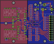
Hi again, I've updated the design to allow a bit of flexibility with input capacitance and impedance also some adjustment of gain for the first op amp. I've still not decided on cap types for the RIAA filters. The RCA connector I've chosen has a 'shunted' pin, I think it's shorted agains the +pin and opens when something is plugged in, I didn't really know what to do with it so I've connected it to ground via a resistor.
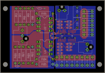
The crappy graphics output makes it look as though there are shorts on the board but I've run a DRC and it looks fine.
Any comments / advice would be very welcome.
Thanks,
Simon.
The crappy graphics output makes it look as though there are shorts on the board but I've run a DRC and it looks fine.
Any comments / advice would be very welcome.
Thanks,
Simon.
Attachments
The crappy graphics output makes it look as though there are shorts on the board but I've run a DRC and it looks fine.
Try a different Gerber viewer before pulling the trigger.
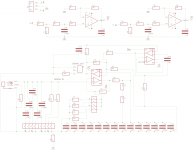
Hi, thanks for the help so far, I ended up going for 1% ceramics on the RIAA filters in the end.
I've made up two of the boards and the RIAA is pretty tight, however I'm getting strange DC offset on the outputs. One board is giving me about 60mV offset no matter what I set the gain to and the other gives me about 25mV at 24dB gain and about 0.7V at 55dB gain.
I've inspected both boards and the components are correctly placed... I did have a bit of trouble with bridging when I was soldering the OPA1652s so there's a possibility I overheated them whilst removing the excess solder.
I've simulated the circuit in TinaTI and the DC analysis comes up with 300uV DC on the output - although I didn't include any of the parasitic characteristics of the layout.
Any advice on how I can go about troubleshooting this would be great...
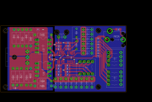
Here's the latest schematic and layout.
Thanks.
I've made up two of the boards and the RIAA is pretty tight, however I'm getting strange DC offset on the outputs. One board is giving me about 60mV offset no matter what I set the gain to and the other gives me about 25mV at 24dB gain and about 0.7V at 55dB gain.
I've inspected both boards and the components are correctly placed... I did have a bit of trouble with bridging when I was soldering the OPA1652s so there's a possibility I overheated them whilst removing the excess solder.
I've simulated the circuit in TinaTI and the DC analysis comes up with 300uV DC on the output - although I didn't include any of the parasitic characteristics of the layout.
Any advice on how I can go about troubleshooting this would be great...
Here's the latest schematic and layout.
Thanks.
Attachments
One board is giving me about 60mV offset no matter what I set the gain to
and the other gives me about 25mV at 24dB gain and about 0.7V at 55dB gain.
The constant 60mV output offset must be from the output stage.
The 0.7V output offset scales with the gain, so it's from the input stage
if that is where you are changing the gain.
Bear in mind that the input offset spec for this part is up to 1.5mV.
At 55dB gain, that's up to 843mV output offset, so this device is not
very well suited for this circuit.
Can you swap the op amps between boards, to see if the offset follows the ICs?
Maybe you can find one IC that has lower offset than the others and use it for the input.
Last edited:
The constant 60mV output offset must be from the output stage.
The 0.7V output offset scales with the gain, so it's from the input stage
if that is where you are changing the gain.
Thanks, that makes sense - gives me something to go on... I'm going to have difficulty removing the ICs as I don't have a hot air gun - although I'm always looking for excuses to buy more kit.
I was hoping the servo would remove the DC at the output stage, I think I'll go back to the data sheets and see if I can make better choices of component.
I was hoping the servo would remove the DC at the output stage.
If you are using the servo, it should be able to null this amount of offset.
Check to make sure it's functioning. It appears there's a missing resistor
from the servo inverting input to ground.
Last edited:
- Status
- This old topic is closed. If you want to reopen this topic, contact a moderator using the "Report Post" button.
- Home
- Source & Line
- Analogue Source
- LME49710 Phono Stage