Hello,
Could you please have a look at these schematics and let me know if I've done it correctly? I need to build a SE to BAL circuit and I started from Rod Elliott's Balanced Transmitter and Receiver II

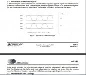
But I need to incorporate this kind of filter:

It is a typical buffer for ADC chips. It's supposed to present very low output impedance at audio frequencies which progressively increases towards to sampling frequency. So I made up this schematic:
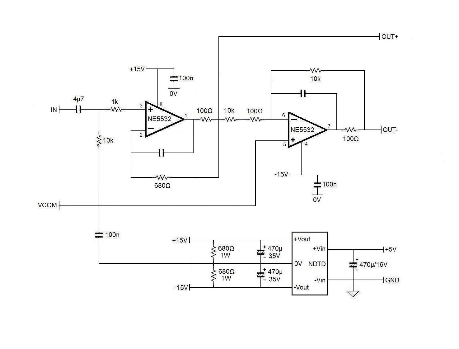
The idea is to keep unity gain and balance. Do you think this would work or has any disadvantages that defeat the purpose?
Could you please have a look at these schematics and let me know if I've done it correctly? I need to build a SE to BAL circuit and I started from Rod Elliott's Balanced Transmitter and Receiver II
But I need to incorporate this kind of filter:
It is a typical buffer for ADC chips. It's supposed to present very low output impedance at audio frequencies which progressively increases towards to sampling frequency. So I made up this schematic:
The idea is to keep unity gain and balance. Do you think this would work or has any disadvantages that defeat the purpose?
Attachments


My first question is, why do you want balanced? Is it for interconnection across a balanced signal interface or, is it because the next stage requires differential drive? Balanced is not necessarily synonymous with differential.
Hi Ken,
Yes it is a buffer to drive an ADC with balanced inputs. Perhaps I should have asked in the digital line level section as the whole design stands on the chip. Anyway, I'll elaborate a little more on this.
Typical schematics for this application show a buffer consisting of one non inverting stage per input phase that either take balanced signal or SE on one phase and the other just buffered at Vcom. Vcom, for those that are not familiar - myself taking my first steps on this- is ADC's internal reference voltage, half the power supply voltage. SE to BAL is what I'm looking for, but done in a way that it will drive the ADC at full digital scale. So, I hope this answers your question.
There are other considerations that I'm sure you are aware of, I'll just list what I've found. Application notes suggest to put a capacitor across the ADC balanced inputs that is necessary for the switching capacitor inside the chip. This external capacitor must then be isolated from the opamp with a resistor but the time constant should be kept low for low distortion. The last schematic in post #1 is supposed to combine all the above. On a second read I realized that the trick with the output resistor in the feedback loop has a meaning when the stage provides gain more than one. If I understand correctly, at unity gain the output impedance will always be equal to the output resistor? Still, if we take the output resistor out of the loop and keep the feedback resistor in parallel with the filter capacitor does it work the way I draw it?
There is another question about Vcom. I'm using an isolated DC-DC converter to supply the opamps separately from the ADC and I was thinking to connect Vcom and the opamps' reference inputs directly to the converter's 0V without the capacitor seen in my schematic. Is this right, or is it dangerous?
You might consider using Linear technologies LT6350. Your app is exactly what it is designed for.
I have a design that required three channels of A/D and very little board space. I don't believe i could have fit if I had used op-amp circuitry.
I have a design that required three channels of A/D and very little board space. I don't believe i could have fit if I had used op-amp circuitry.
Thanks, very interesting! For future projects though. For now I'm stuck with +/-15V and most likely I'm going to use external resistors to control gain anyway. But definitely something to keep in mind!
I strongly suggest exactly copying one of the application circuits published by the one of the chip vendors. Check the datasheet for the ADC you're interfacing to. If it contains such an application circuit, I would clone it.
As far as the isolated op-amp power supply is concerned, you need to un-isolate it. It needs to share a common reference (signal ground) with the input signal. As it appears designed, the signal and the op-amp supply are floating, with respect to each other.
Bypass that 100nF icap., and connect the +/- 15V isolated supply 0V terminal to signal ground. Also, connect the 10K input resistor to signal ground. However, first, be certain that the +/- 15V supply's output is actually isolated from it's 5V input.
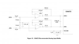
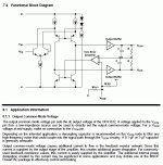
Here's some more info on this. The chip is CS4272. Attached is the datasheet and a pic of page 32.http://www.mouser.com/ds/2/76/cs4272_f1-43250.pdf In general, the common practice is to design buffer stages as an extension of the ADC internal structure. Thus, it is strongly recommended to supply both ADC and buffer from the same source and DC coupling using the ADC's internal reference voltage (Vcom) -usually half rail. The ADC and the buffer use Vcom as a virtual ground. It seems that this is the only way to achieve low distortion.
I've tried input buffer referenced to ground and to Vcom both AC and DC coupled. Best results with Vcom and DC coupling as the datasheet suggests but but with 5V rail it will never reach 5,6Vpp for 0dBFS. So, I've built a prototype with +/-15V with an isolated DC booster which currently works with in-out grounds shorted and the capacitor between 0V and Vcom (see first post). Good so far but not the best. The DC booster is completely floating and I thought it would be better to attach it directly to Vcom -bridge the cap- taking advantage of the isolation feature.
I've tried input buffer referenced to ground and to Vcom both AC and DC coupled. Best results with Vcom and DC coupling as the datasheet suggests but but with 5V rail it will never reach 5,6Vpp for 0dBFS. So, I've built a prototype with +/-15V with an isolated DC booster which currently works with in-out grounds shorted and the capacitor between 0V and Vcom (see first post). Good so far but not the best. The DC booster is completely floating and I thought it would be better to attach it directly to Vcom -bridge the cap- taking advantage of the isolation feature.
Attachments

Last edited:
I see your trouble. With your circuit, input signal will undesirably modulate VCOM to some degree via the 10k input resistor, which connects the two. To fully fix this issue may require resort to two separate VCOM buffers.
I suggest instead giving serious consideration to regulating the +/- 15V supply down to a voltage low enough to use one of the specialized single-ended to differential amplifiers, such as was mentioned above.
I suggest instead giving serious consideration to regulating the +/- 15V supply down to a voltage low enough to use one of the specialized single-ended to differential amplifiers, such as was mentioned above.
Last edited:
Bus, check out the T.I. OPA1632.
I seems to meet all of you requirements. It's a differential in to differential out, very low THD op-amp designed specifically for driving differential input ADC chips. Figure 13, of the data sheet shows an implementation of the device for converting single-ended input to differential output. If also features a dedicated VCOM input to greatly simplify establishing the needed common-mode D.C. offset of the differential outputs. It will accept up to +/- 16V supply rails, enabling you to utilize your existing 15V supply without change.
http://www.ti.com/lit/ds/symlink/opa1632.pdf
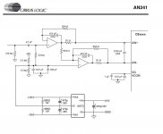
Thanks Ken! Indeed, how to refer the circuit to Vcom is what bothers me at the moment. OPA1632 seems a very good option. In the suggested schematic they seem to spot the problem and solve it with a buffer. I'll keep it in mind. Meanwhile, I found this paper https://d3uzseaevmutz1.cloudfront.net/pubs/appNote/an241-1.pdf where at page #5 it gives a schematic with opamps with a very nice explanation. They avoid Vcom - I guess they know better about their chips- and use a voltage divider, ordinary application for single rail supply. And with anti-aliasing filter... and for CS4272! But, as I said I need more voltage swing than 5V, so I built a prototype based on the attached schematic with isolated grounds for the DC booster. Most likely to be ready for test tonight. I'll be back.
Attachments
Thanks Ken! Indeed, how to refer the circuit to Vcom is what bothers me at the moment. OPA1632 seems a very good option. In the suggested schematic they seem to spot the problem and solve it with a buffer...
I saw that, and thought it odd that VCOM pin would require buffering. The OPA1632 data sheet specifies all input pins as having an input impedance of 34 Meg, which I assume includes the VCOM pin.
Another option is to use low voltage opamps such as the opa836 in inverting configuration. I once sketched something gathered from various datasheets and app notes here: USB powered ADC (pcm4202-cs8406)
One more project that didn't go anywhere...
One more project that didn't go anywhere...
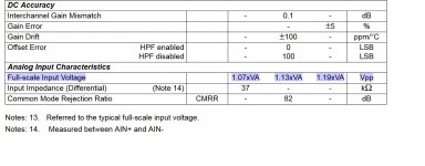
I am confused... I can't see 5,64Vpp here. How could it be so with single rail 5V and Vcom=2,5V? Is it only me who sees 2,82Vpp?

But then it says full scale input voltage = 1,13*VA. What does this mean? For VA=5V it will be 5,65Vpp and for VA=4,5V 5,085Vpp? It always split VA in half to get Vcom and in real life I have VA=4,6V, Vcom=2,3V and it doesn't go to 0dB with full 4,6V rail swing and even more.
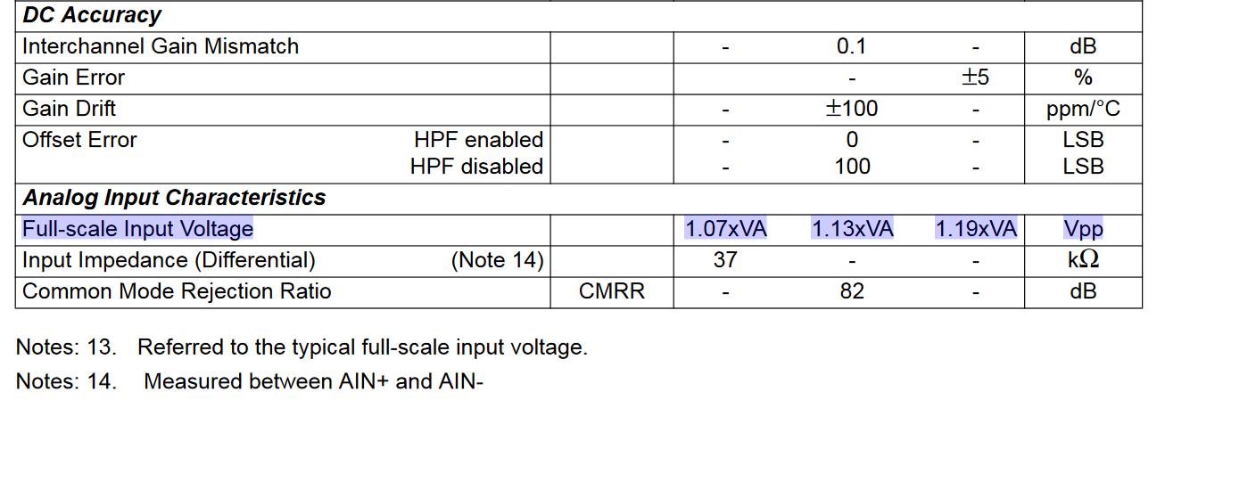
So, it needs 5,65Vpp input no matter what supply voltage and it simply cannot reach 0dBFS?
But then it says full scale input voltage = 1,13*VA. What does this mean? For VA=5V it will be 5,65Vpp and for VA=4,5V 5,085Vpp? It always split VA in half to get Vcom and in real life I have VA=4,6V, Vcom=2,3V and it doesn't go to 0dB with full 4,6V rail swing and even more.
So, it needs 5,65Vpp input no matter what supply voltage and it simply cannot reach 0dBFS?
Attachments
I saw that, and thought it odd that VCOM pin would require buffering. The OPA1632 data sheet specifies all input pins as having an input impedance of 34 Meg, which I assume includes the VCOM pin.
Data sheet details clearly show a pair of 30k resistors off Vocm and speak of a "low impedance source" to force it off half-supply.
Attachments
I am confused... I can't see 5,64Vpp here. How could it be so with single rail 5V and Vcom=2,5V? Is it only me who sees 2,82Vpp?
2.82Vpp but it's differential 😉 ... so twice that as explained in the datasheet
So, 5V supply is enough for this? And what would be the meaning for any higher. With Vcom=2,5V the lower part of the voltage swing is restricted to that. What do I miss?
Yes, 5V is enough, provided the circuit can swing down to 1.09V and up to 3.91V.
Think about it. In 6Vpp single ended signal (I'm rounding up), the signal is up to 3V away from the reference, once up, once down. In a differential signal, this same 3V difference can be achieved by moving both + and - 1.5V away from Vcom.
Think about it. In 6Vpp single ended signal (I'm rounding up), the signal is up to 3V away from the reference, once up, once down. In a differential signal, this same 3V difference can be achieved by moving both + and - 1.5V away from Vcom.
Data sheet details clearly show a pair of 30k resistors off Vocm and speak of a "low impedance source" to force it off half-supply.
Yup, you're correct. VCOM's input impedance is no higher than 15K. I should have thought to see the data sheet's simplified internal schematic diagram.
It was a good thing to bring my queries in this thread! Your replies helped to find my way. I mistakenly, thought that the ADC couldn't be driven to full scale because of psu rail headroom. VA*1,13 tested from 4,7V to 5,5V is able to achieve that. The culprit was else. You can read more about this here Behringer UMC 202HD for measurements
One word about the active filter in the analog domain. It is recommended but at least for this converter is kind of academical. I couldn't see any difference with and without it. The built-in digital antialiasing filter seems to do all the job.
One word about the active filter in the analog domain. It is recommended but at least for this converter is kind of academical. I couldn't see any difference with and without it. The built-in digital antialiasing filter seems to do all the job.
- Status
- Not open for further replies.
- Home
- Source & Line
- Analog Line Level
- SE to BAL conversion with active filter